SBX-5363 AMD Geode 3.5" Embedded Board User's Manual Version 1.0 2009.
Index Table of Contents Chapter 1 Introduction ............................................. 1 1.1 Copyright Notice ........................................................ 1.2 About this User's Manual ............................................. 1.3 Warning ..................................................................... 1.4 Replacing the lithium battery ....................................... 1.5 Technical Support ....................................................... 1.6 Warranty ................
Index Chapter 3 BIOS ......................................................... 22 3.1 BIOS Introduction ....................................................... 23 3.2 BIOS Setup ................................................................ 23 3.3 Standard CMOS Features ............................................ 24 3.4 Advanced BIOS Features ............................................. 26 3.5 Advanced Chipset Features ......................................... 28 3.6 Integrated Peripherals ............
Introduction 1 Chapter 1 Introduction -1-
Introduction 1.1 Copyright Notice All Rights Reserved. The information in this document is subject to change without prior notice in order to improve the reliability, design and function. It does not represent a commitment on the part of the manufacturer. Under no circumstances will the manufacturer be liable for any direct, indirect, special, incidental, or consequential damages arising from the use or inability to use the product or documentation, even if advised of the possibility of such damages.
Introduction 1.4 Replacing the lithium battery Incorrect replacement of the lithium battery may lead to a risk of explosion. The lithium battery must be replaced with an identical battery or a battery type recommended by the manufacturer. Do not throw lithium batteries into the trashcan. It must be disposed of in accordance with local requlations concerning special waste. 1.
Introduction 1.6 Warranty This product is warranted to be in good working order for a period of two years from the date of purchase. Should this product fail to be in good working order at any time during this period, we will, at our option, replace or repair it at no additional charge except as set forth in the following terms. This warranty does not apply to products damaged by misuse, modifications, accident or disaster.
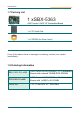
Introduction 1.7 Packing List 1 xSBX-5363 AMD Geode LX800 3.5" Embedded Board 1 x CPU Heat Sink 1 x CDROM (for Driver Used) If any of the above items is damaged or missing, contact your vendor immediately. 1.8 Ordering Information SBX-5363-R/ Lx800 AMD Geode LX800(500MHz) 3.5 Embedded Board with onboard 256MB DDR SDRAM SBX-5363-S/Lx800 AMD Geode LX800(500MHz) 3.
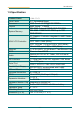
Introduction 1.9 Specification Product Name Form Factor Processor Chipset System Memory SBX-5363 3.5" Embedded Board AMD Geode LX 800@0.
Introduction 1.
Introduction USB1 LAN KB/MS RES JBAT1 VGA USB2 COM1 AUDIO HDD LED Power LED AMD Cs5536 PC/104 DDR SDRAM AMD Lx800 DIO LPD/FDD JCF1/JVLCD1 COM2 Main Power .
Installation 2 Chapter 2 Installation -9-
Installation 2.1 Jumpers Quick Reference Jumpers Label JBAT1 JCF1 JRS1 JVLCD1 Function Clear CMOS CF master or slave selected RS-232 / 422 / 485 Selection LCD Voltage Selected 2.1.1 CMOS Jumper Settings Type: Onboard 3-pin header (JBAT1) CMOS Setup (JBAT1) Keep CMOS (default setting) Clear CMOS JBAT1 1-2 ON 2-3 ON JBAT1 2.1.
Installation 2.1.3 Serial Port Select RS-232C/422/485 Mode select (JRS1) RS-232C/422/485 Mode on COM2 The onboard COM2 port can be configured to operate in RS-422 or RS-485 modes. RS-422 modes differ in the way RX/TX is being handled. Jumper JRS1 switches between RS-232 or RS-422/485 mode. When JRS1 is set to RS-422 or 485 mode, there will be only +12V output left while JRS1 is set. All of the RS232/422/485 modes are available on COM2.
Installation 2.
Installation 2.2.1 Ethernet Connector Connector: LAN1 Type: One external RJ-45 on bracket Pin 1 3 5 7 Description Tx+ Rx+ NC NC Pin 2 4 6 8 Description TxNC RxNC 2.2.
Installation 2.2.
Installation 2.2.4 Flat Panel Connector LCD Interface Connector LCD1 connector is defined for TTL panel supporting up to 24-bit. LCD2 connector is defined for LVDS panel supporting 18-bit only. Connector: LCD1 Type: One onboard DF13-40DS Header Pin 1 3 5 7 9 11 13 15 17 19 21 23 25 27 29 31 33 35 37 39 Description VDD GND 3.
Installation Connector: LVDS1 Type: One onboard DF13-30DS Header Pin 1 3 5 7 9 11 13 15 17 19 21 23 25 27 29 Description VDD LVDS CLK+ LVDS CLKGND LVDS TX0+ LVDS TX0GND LVDS TX1+ LVDS TX1GND LVDS TX2+ LVDS TX2GND LVDS TX3+ LVDS TX3- Pin 2 4 6 8 10 12 14 16 18 20 22 24 26 28 30 Description NC NC NC NC NC NC NC NC NC NC NC NC NC NC NC LVDS1 LVDS Panel Inverter Connector: INV1 Type: One onboard 1x5pin Wafer Header Pin 1 2 3 4 5 Description +12V GND Backlight on/off Brightness control GND INV1 - 16 -
Installation 2.3 Peripheral Ports 2.3.1 Parallel Port (Share with FDD) Connector: LPT1 Type: One onboard 2x10Pin Header Pin 1 3 5 7 9 11 13 15 17 19 Description #STB PD0 PD1 PD2 PD3 PD4 PD5 PD6 PD7 #ACK Pin 2 4 6 8 10 12 14 16 18 20 Description #AFD #ERR #INIT #SLIN GND GND NC BUSY PE SLCT LPT1 2.3.
Installation 2.3.3 PS/2 Keyboard & Mouse Connector: KBM1 Type: One external 6-pin Mini DIN connector on bracket Pin 1 3 5 Description KB_DATA GND KB_CLK Pin 2 4 6 Description MS_DATA +5V MS-CLK 2.3.4 CRT Display Connector Connector: VGA1 Type: One external 15-pin D-sub female connector on bracket Pin 1 3 5 7 9 11 13 15 Description RED BLUE GND GND VCC NC HSYNC VDCLK Pin 2 4 6 8 10 12 14 Description GREEN NC GND GND GND VDDAT VSYNC 2.3.
Installation 2.3.
Installation 2.3.7 Audio Interface Port Connector: AUDIO1 Type: One onboard 2x5pin Box Header Pin 1 3 5 7 9 Description LINEL MIC GND AGND LOUT-L Pin 2 4 6 8 10 Description LINER GND NC AGND LOUT-R AUDIO1 2.3.
Installation 2.
BIOS 3 Chapter 3 BIOS - 22 -
BIOS 3.1 BIOS Introduction The Award BIOS (Basic Input/Output System) installed in your computer system's. The BIOS provides for a standard device such as disk drives, serial ports and parallel ports. It also adds password protection as well as special support for detailed fine-tuning of the chipset controlling the entire system. 3.2 BIOS Setup The Award BIOS provides a Setup utility program for specifying the system configurations and settings. The BIOS ROM of the system stores the Setup utility.
BIOS 3.3 Standard CMOS Features "Standard CMOS Features" allows you to record some basic hardware configurations in your computer system and set the system clock and error handling. If the CPU card is already installed in a working system, you will not need to select this option. You will need to run the Standard CMOS option, however, if you change your system hardware configurations, such as onboard battery fails, or the configuration stored in the CMOS memory was lost or damaged.
BIOS IDE Primary HDDs / IDE Secondary HDDs The onboard PCI IDE connectors provide Primary and Secondary channels for connecting up to four IDE hard disks or other IDE devices. Each channel can support up to two hard disks; the first is the "Master" and the second is the "Slave". Press to configure the hard disk. The selections include Auto, Manual, and None. Select 'Manual' to define the drive information manually. You will be asked to enter the following items.
BIOS Halt On This field determines whether or not the system will halt if an error is detected during power up. All errors (default) Whenever the BIOS detects a non-fatal error, the system will stop and you will be prompted. No errors The system boot will not be halted for any error that may be detected. All, But Keyboard The system boot will not be halted for a keyboard error; it will stop for all other errors.
BIOS First/ Second/Third Boot Device These fields determine the drive that the system searches first for an operating system. The options available include Setting: Floppy, LS-120, HDD-0, SCSI, CDROM, HDD-1, ZIP100, USB-FDD, USB-ZIP, USB-CDROM, USB-HDD, LAN and Disabled. Boot Other Device It allows the system to search for an OS from other devices other than the ones selected in the First/ Second/ Third Boot Device. Setting: Disabled/ Enabled (Default).
BIOS 3.5 Advanced Chipset Features CAS Latency It allows CAS latency time in HCLKs. The system board designer should set the values in this field, depending on the DRAM installed. Do not change the values in this field unless you change specifications of the installed DRAM or CPU. Setting: Auto (Default)/1.5/2.0/2.5/3.0/3.5. Interleave Select It allows you to Use the Interleave Select option to specify how the cache memory is interleaved. Setting: LOI (Default)/HOI.
BIOS XOR Bit Select Setting: 18(Default)/19/20/21. Video Memory Size In order to determine how much memory is allocated to the video graphics device. Setting: None/8M(Default)/16M/32M/64M/128M/254M. Output display In order to specify the display devices the system is connected to. Setting: Flat Panel/CRT (Default)/Panel & CRT. Flat Panel Configuration It allows you to open the Flat Panel Configuration menu.
BIOS 3.6 Integrated Peripherals On-Chip IDE Device >>> On-Chip IDE Channel 1 The integrated peripheral controller contains an IDE interface with support for two IDE channels. Select Enabled to activate each channel separately. Setting: Disabled/Enabled (Default). Master/Slave Drive PIO Mode It allows your system HDD controller to run faster.
BIOS IDE Primary Master/Slave UDMA It allows your system to improve disk I/O throughput to 33MB/sec with the Ultra DMA33 feature. Setting: Disabled/Auto (Default). IDE DMA Transfer Access Setting: Disabled, Enabled (Default). IDE HDD Block Mode It allows HDD controller to use the fast block mode to transfer data to and from HDD. Setting: Disabled/Enabled (Default).
BIOS Onboard Serial/Parallel Port It allows you to select the onboard serial and parallel ports with their addresses. Setting: Serial Port 1 3F8/IRQ4 (Default) Serial Port 2 2F8/IRQ3 (Default) Parallel Port 378/IRQ7 (Default) UART Mode Select It determines the UART 2 mode in your computer. Setting: IrDA/ASKIR/Normal (Default). RxD, TxD Active Setting: Hi, Hi/Hi, Lo (Default)/Lo, Hi /Lo, Lo. IR Transmission Delay Setting: Disabled/Enabled (Default). UR2 Duplex Mode Setting: Full/Half (Default).
BIOS Serial Port 3 Use IRQ Setting: IRQ10 (Default)/IRQ11. Serial Port 4 Use IRQ Setting: IRQ10 /IRQ11 (Default). IT8888 ISA Decode IO >>> It allows you to use the IT8888 ISA Decode IO menu to set the IO memory range for the onboard ISA. Decode I/O Space 0/ 1/ 2/ 3/ 4/ 5 It allows you to allocate system resources to the ISA bridge and to enable the function correctly. Setting: Disabled, Enabled (Default). Decode I/O Speed 0/ 1/ 2/ 3/ 4/ 5 It allows you to specify the speed of the ISA bus.
BIOS Decode I/O Size 0/ 1/ 2/ 3/ 4/ 5 It allows you to specify the size of the ISA bus. Setting: 1 Byte, 2 Bytes, 4 Bytes, 8 Bytes, 16 Bytes, 32 Bytes, 64 Bytes, 128 Bytes. IT8888 ISA Decode Memory >>> It allows you to use the IT8888 ISA Decode Memory to set the resources for the onboard ISA bus. Decode Memory Space 0/ 1/ 2/ 3 It allows you to allocate memory resources to the ISA bridge and to enable the function correctly. Setting: Disabled (Default), Enabled.
BIOS IT8888 DDMA >>> Suppose that the ISA bus card is required DMA1 & DMA5. Set "DDMA1 Support" & "DDMA5Support" to "Enabled". Onboard Audio Setting: Enabled (Default), Disabled. 3.7 Power Management Setup ACPI Function It supports ACPI (Advance Configuration and Power Interface). Setting: Enabled (Default) /Disabled.
BIOS Power Management It allows you to select the type of power saving management modes. Setting: APM Advanced power management (APM) ACPI (Default) Advanced Configuration and Power Interface (ACPI) Modem Use IRQ It sets the IRQ used by the Modem. Setting: N/A (Default)/3/4/5/7/9/10/11. PME Event Function Setting: Disabled/Enabled (Default). Soft-Off by PWR-BTTN It defines the power-off mode when using an ATX power supply.
BIOS 3.8 PNP/PCI Configurations PNP OS Installed It allows you to enable the PNP OS Install option if it is supported by the OS installed. Setting: No (Default) /Yes. Reset Configuration Data It allows you to determine whether to reset the con?guration data or not. Setting: Disabled (Default) /Enabled. Resources Controlled By This PnP BIOS can configure all of the boot and compatible devices with the use of a PnP operating system. Setting: Auto (ESCD) (Default) /Manual.
BIOS PCI/VGA Palette Snoop Some non-standard VGA display cards may not show colors properly. It allows you to set whether or not MPEG ISA/VESA VGA cards can display with PCI/VGA. When "Enabled", a PCI/VGA can display with an MPEG ISA/VESA VGA card. When "Disabled", a PCI/VGA cannot display with an MPEG ISA/VESA VGA card. Setting: Disabled (Default) /Enabled. 3.
BIOS 3.10 Load Optimized Defaults It allows you to load the default values to your system configuration. The default setting is optimal and enabled all high performance features. 3.
BIOS Useing Password to set a password that will be used exclusively on the system. To specify a password, highlight the type you want and press . The Enter Password: message prompts on the screen. Type the password, up to eight characters in length, and press . And the system confirms your password by asking you to type it again. After setting a password, the screen automatically returns to the main screen.
BIOS 3.13 Exit Without Saving Typing 'Y" will quit the Setup utility without saving the modifications. Typing "N" will return you to Setup utility. 3.
BIOS 3.15 BIOS memory mapping Address Device E000:0000h - F000:FFFFh D000:2000h - D000:FFFFh D000:0000h - D000:1FFFh C000:E000h - CF00:FFFFh C000:0000h - C000:DFFFh A000:0000h - B000:FFFFh 0000:0000h - 9000:FFFFh Description System BIOS Area Free space LAN ROM Free space VGA BIOS VGA RAM DOS 640K 3.
BIOS 0Eh Test F000h segment shadow to see whether it is read/write capable or not. If test fails, keep beeping the speaker 0Fh Reserved 10h Auto detect flash type to load appropriate flash read/write codes into the run time area in F000 for ESCD & DMI support 11h Reserved 12h Use walking 1's algorithm to check out interface in CMOS circuitry. Also set real time clock power status and then check for overrride 13h Reserved 14h Program chipset default values into chipset.
BIOS 24h 25h 26h 27h 28h 29h 2Ah 2Bh 2Ch 2Dh Eh 2Fh 30h 31h 32h 33h 34h 35h 36h 37h 38h 39h 3Ah 3Bh 3Ch 3Dh 3Eh 3Fh 40h 41h 42h 43h 44h Reserved Reserved Reserved Initialize INT 09 buffer Reserved Program CPU internal MTRR (P6 & PII) for 0-640K memory address; Initialize the APIC for Pentium class CPU; Program early chipset according to CMOS setup; Measure CPU speed; Invoke video BIOS Reserved Reserved Reserved Initialize multilanguage; Put information on screen display, including Award title, CPU type,
BIOS 45h 46h 47h 48h 49h 4Ah 4Bh 4Ch 4Dh 4Eh 4Fh 50h 51h 52h 53h 54h 55h 56h 57h 58h 59h 5Ah 5Bh 5Ch 5Dh 5Eh 5Fh 60h 61h Reserved Reserved Initialize EISA slot Reserved Calculate total memory by testing the last double last word of each 64K page; Program writes allocation for AMD K5 CPU Reserved Reserved Reserved Reserved Program MTRR of M1 CPU; initialize L2 cache for P6 class CPU & program cacheable range; Initialize the APIC for P6 class CPU; On MP platform, adjust the cacheable range to smaller one i
BIOS 62h 63h 64h 65h 66h 67h 68h 69h 6Ah 6Bh 6Ch 6Dh 6Eh 6Fh 70h 71h 72h 73h 74h 75h 76h 77h 78h 79h 7Ah 7Bh 7Ch 7Dh 7Eh 7Fh Reserved Reserved Reserved Initialize PS/2 mouse Reserved Prepare memory size information for function call: INT 15h ax=E820h Reserved Turn on L2 cache Reserved Program chipset registers according to items described in Setup & Auto-Configuration table Reserved Assign resources to all ISA PnP devices; Auto assign ports to onboard COM ports if the corresponding item in Setup is set t
BIOS Reserved Reserved Call chipset power management hook: Recover the text fond usedby EPA logo (not for full screen logo), If password is set, ask for password 83h Save all data in stack back to CMOS 84h Initialize ISA PnP boot devices 85h Final USB initialization; NET PC: Build SYSID structure; Switch screen back to text mode; Set up ACPI table at top of memory; Invoke ISA adapter ROM's; Assign IRQ's to PCI devices; Initialize APM; Clear noise of IRQ's 86h Reserved 87h Reserved 88h Reserved 89h Reserved
Appendix 4 Chapter 4 Appendix - 48 -
Appendix 4.1 I/O Port Address Map Each peripheral device in the system is assigned a set of I/O port addresses which also becomes the identity of the device. The following table lists the I/O port addresses used.
Appendix 00000170 - 00000177 000001F0 - 000001F7 00000274 - 00000277 00000279 - 00000279 000002F8 - 000002FF 00000376 - 00000376 00000378 - 0000037F 000003B0 - 000003BA 000003C0 - 000003DF 000003F0 - 000003F5 000003F6 - 000003F6 000003F7 - 000003F7 000003F8 - 000003FF 00000778 - 0000077B 00000D00 - 0000AC17 0000AC20 - 0000FFFF 0000E000 - 0000EFFF 0000FD00 - 0000FD7F 0000FE00 - 0000FE0F 0000FF00 - 0000FF3F Secondary IDE Channel Primary IDE Channel ISAPNP Read Data Port ISAPNP Read Data Port Communications
Appendix 4.2 Interrupt Request Lines (IRQ) Peripheral devices use interrupt request lines to notify CPU for the service required. The following table shows the IRQ used by the devices on board.