
Specification Sheet
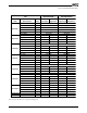


PID: 43375 Rev 3.46 - September 2010 AMD Family 10h Desktop Processor
Power and Thermal Data Sheet
60AMD Phenom™ Processor
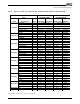
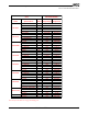
AMD Phenom™ Processor Thermal and Power Specification Table Notes:
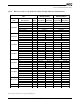
1. Tcase Max is the maximum case temperature specification which is a physical value in degrees
Celsius. Tcase Max can be any valid Tcase Max value in the range specified for the corresponding
OPN.
2. Tctl Max (maximum control temperature) is a non-physical temperature on an arbitrary scale that can be
used for system thermal management policies. Refer to the
BIOS and Kernel Developer’s Guide (BKDG)
for AMD Family 10h Processors, order# 31116.
3. The processor thermal solution should be designed to accommodate thermal design power (TDP) at
Tcase Max. TDP is measured under the conditions of all cores operating at CPU COF, Tcase Max, and
VDD at the voltage requested by the processor. TDP includes all power dissipated on-die from VDD,
VDDNB, VDDIO, VLDT, VTT, and VDDA. TDP is not the maximum power of the processor.
4. P-state limit when HTC is active. Refer to the BIOS and Kernel Developer’s Guide (BKDG) for AMD
Family 10h Processors, order# 31116 for more information.
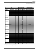
5. Hardware transitions the part to startup P-state at cold boot. During initialization, the startup NB COF
and VID_VDDNB values may differ from those of the startup P-state. Please see the BIOS and Kernel
Developer's Guide (BKDG) for AMD Family 10h Processors, order# 31116 for detailed power sequencing
information.
6. Frequency reported to the OS is rounded to the nearest 100-MHz boundary.
7. During initialization, the startup NB COF and VID_VDDNB values may differ from those of the startup
P-state. Please see the BIOS and Kernel Developer’s Guide (BKDG) For AMD Family 10h Processors,
order# 31116 for specific power sequencing information.
8. Specifications for multi-core processors assume equivalent P-states (voltage and frequency) and
equivalent Tcase conditions for all cores. Refer to the BIOS and Kernel Developer’s Guide (BKDG) for
AMD Family 10h Processors, order #31116, for details on P-state operation for multi-core processors.
9. Variable voltage, any valid voltage between VID_VDD Min and VID_VDD Max is allowed.
10. TDP IDD conditions: single-plane platforms supply IDD and IDDNB tied together and use the IDD Max
specification.
11. Single-plane platforms have VID_VDD and VID_VDDNB tied together, and use the VID_VDD
specification.
12. TDP IDDNB conditions: single-plane platforms supply IDD and IDDNB tied together and use the IDDNB
Max specification.
13. Thermal Design Power dissipated by the processor VDDIO and VTT power planes only. Assumes
VDDIO = 1.8 V and VTT = VDDIO / 2.
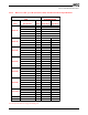
14. Refer to erratum 308 in the Revision Guide for AMD Family 10h Processors, order# 41322 for the
appropriate clock divisor setting.
15. Assumes 50°C, Min P-state VID_VDD, core clock divider set to 128, and L2 and data cache scrubbing
disabled. Refer to the BIOS and Kernel Developer's Guide (BKDG) for AMD Family 10h Processors,
order# 31116 for recommended settings.
16. Assumes 35°C, min P-state VID_VDD, core clock divider set to 16, HyperTransport™ link s
disconnected, memory in self-refresh mode, and DDR2 SDRAM interface tristated. Recommended
settings in the BIOS and Kernel Developer's Guide (BKDG) for AMD Family 10h Processors, order#
31116, provide improved power values.
17. Thermal Design Power dissipated by the processor at min P-state VID_VDDNB.
18. Thermal Design Power dissipated by the processor at min P-state VID_VDD.
19. This product is recommended for dual-plane platforms only.
20. Core Power (Pre-Flush) and (Post-Flush) refers to the Cache Flush On Halt feature described in the
BIOS and Kernel Developer’s Guide (BKDG) for AMD Family 10h Processors, order# 31116. Core Power
pre-flush and post-flush values are based on the recommended BKDG settings. Actual C1 idle core
power varies with system usage according to the following equation:
C1 idle Core Power = F3xDC[CashFlushOnHaltTmr]/OS timer tick interval * Core Power (Pre-Flush) +
(1 - F3xDC[CachFlushOnHaltTmr]/OS timer tick interval * Core Power (Post-Flush))
The default Microsoft
®
Windows Vista
®
timer tick interval is 15.6 ms. This interval varies between
operating systems and within an operating system depending on usage.
21. Valid for dual-plane operation only.