
Specifications


SLAS495A− JUNE 2006 − REVISED OCTOBER 2007
www.ti.com
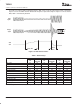
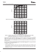
30
−20
−18
−16
−14
−12
−10
−8
−6
−4
−2
0
0 200 400 600 800 1000
f − Frequency − Hz
Gain − dB
Figure 20. Uncompensated Response For 16-Ω Load and 50-mF Decoupling Capacitor
−20
−18
−16
−14
−12
−10
−8
−6
−4
−2
0
0
200 400 600 800 1000
f − Frequency − Hz
Gain − dB
Figure 21. Frequency Response For 16-Ω Load and 50-mF Decoupling Capacitor After Gain
Compensation Using Above Set of Coefficients For Audio Effects Filter
Using the capless output configuration eliminates the need for these capacitors and removes the accompanying
high-pass filter entirely. However, this configuration does have one drawback – if the RETURN terminal of the
headphone jack (which is wired to the TSC2111 VGND pin) is ever connected to a ground that is shorted to the
TSC2111 ground pin, then the VGND amplifier enters short-circuit protection, and the audio output does not
function properly.
The TSC2111 incorporates a programmable short-circuit detection/protection function. In case of short circuit,
all analog outputs are disabled and a read only bit D1 of control register 1DH/page 2 is set. In such cases, there
are two ways to return to normal operation:
− Hardware or software reset
− Power down all the output drivers, which can be achieved by setting bits D12, D11, D 8, D7, and D6 of control
register 05H/page 2 and then wait for driver power down status flags (bits D15−D10 of control register
25H/page 2) to become 1. The wait time is typically less than 50 ms after which, output drivers can be
programmed as desired.