
Specifications


SLAS495A− JUNE 2006 − REVISED OCTOBER 2007
www.ti.com
54
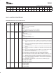
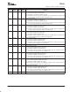
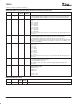
REGISTER 02H: Buffer Control
BIT NAME
RESET
VALUE
READ/
WRITE
FUNCTION
D15 BUFRES 0 R/W Buffer Reset.
0 => Buffer mode is disabled and RDPTR, WRPTR & TGPTR set to their reset value.
1 => Buffer mode is enabled.
D14 BUFCONT 0 R/W Buffer Mode Selection
0 => Continuous conversion mode.
1 => Single shot mode.
D13−D11 BUFTL 000 R/W Trigger Level TL selection of Buffer used for SAR ADC
000 => 8
001 => 16
010 => 24
011 => 32
100 => 40
101 => 48
110 => 56
111 => 64
D10 BUFOVF 0 R Buffer Full Flag
0 => Buffer is not full.
1 => Buffer is full. This means buffer contains 64 unread converted data.
D9 BUFEMF 1 R Buffer Empty Flag
0 => Buffer is not empty.
1 => Buffer is empty. This means there is no unread converted data in the buffer.
D8−D0 0’s R Reserved
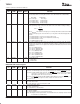
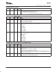
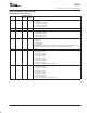
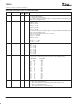
REGISTER 03H: Reference Control
BIT NAME
RESET
VALUE
READ/
WRITE
FUNCTION
D15−D6 0’s R Reserved
D5 0 R/W Reserved. Always write 0 to this bit.
D4 VREFM 0 R/W Voltage Reference Mode. This bit configures the VREF pin as either external reference or internal
reference.
0 => External reference
1 => Internal reference
D3−D2 RPWUDL 00 R/W Reference Power Up Delay. These bits allow for a delay time for measurements to be made after
the reference powers up, thereby assuring that the reference has settled
00 => 0 µs
01 => 100 µs
10 => 500 µs
11 => 1000 µs
Note: This will be valid only when device is programmed for internal reference and Bit D1 = 1, i.e.,
reference is powered down between the conversions if not required.
D1 RPWDN 1 R/W Reference Power Down. This bit controls the power down of the internal reference voltage.
0 => Powered up at all times.
1 => Powered Down between conversions.
Note: When D4 = 0 i.e. device is in external reference mode then the internal reference is powered
down always.
D0 IREFV 0 R/W Internal Reference Voltage. This bit selects the internal voltage for TSC ADC.
0 => VREF = 1.25 V
1 => VREF = 2.50 V