
Specifications


SLAS495A− JUNE 2006 − REVISED OCTOBER 2007
www.ti.com
73
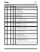
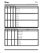
REGISTER 22H: Audio Control 7
BIT NAME
RESET
VALUE
READ/
WRITE
FUNCTION
D15 DETECT 0 R/W Headset Detection
0 => Disable headset detection
1 => Enable headset detection
D14−D13 HESTYPE 00 R Type of Headset Detected.
00 => No headset detected.
01 => Stereo headset detected.
10 => Cellular headset detected
11 => Stereo+cellular headset detected
Note: These two bits are valid only if the headset detection is enabled.
D12 HDDETFL 0 R Headset Detection Flag.
0 => Headset is not detected
1 => Headset is detected.
D11 BDETFL 0 R Button Press Detection Flag.
0 => Button press is not detected
1 => Button press is detected.
D10−D9 HDDEBNPG 01 R/W De−bouncing Programmability for Glitch Rejection During Headset Detection.
00 => 16 ms duration (with 2 ms clock resolution)
01 => 32 ms duration (with 4 ms clock resolution)
10 => 64 ms duration (with 8 ms clock resolution)
11 => 128 ms duration (with 16 ms clock resolution)
D8 0 R Reserved (Write only 0)
D7−D6 BDEBNPG 00 R/W De−bouncing Programmability for Glitch Rejection During Button Press Detection.
00 => No glitch rejection.
01 => 8 ms duration (with 1 ms clock resolution)
10 => 16 ms duration (with 2 ms clock resolution)
11 => 32 ms duration (with 4 ms clock resolution)
D5 0 R Reserved (Write only 0)
D4 DGPIO2 0 R/W Enable GPIO2 for Headset Detection Interrupt
0 => Disable GPIO2 for headset detection interrupt
1 => Enable GPIO2 for headset detection interrupt
Note: This programmability is valid only if D15 and D13 of control register 23H/page 2 are set to
0
D3 DGPIO1 0 R/W Enable GPIO1 for Headset Detection Interrupt
0 => Disable GPIO1 for Detection interrupt
1 => Enable GPIO1 for Detection interrupt
Note: This programmability is valid only if D11 and D9 of control register 23H/page 2 are set to
0
D2 CLKGPIO2 0 R/W Enable GPIO2 for CLKOUT
0 => Disable GPIO2 for CLKOUT mode.
1 => Enable GPIO2 for CLKOUT mode.
In CLKOUT mode the frequency of output signal is equal to the 256xDAC_FS if DAC_FS is faster
than ADC_FS otherwise equal to the 256xADC_FS.
Note: This programmability is valid only if PLL is enabled, D15 and D13 of register 23H/page 2
are set to 0 and GPIO2 is not enabled for detection interrupt.
D1−D0 ADWSF 00 R/W ADWS Selection
0X => GPIO1 pin output is three−stated.
10 => GPIO1 pin acts as button press detect interrupt.
11 => GPIO1 pin acts as ADC word−select (ADWS).
Note: 1. This programmability is valid only if D11 and D9 of control register 23H/page 2 are set
to 0.
2. These bits should be programmed ‘11’ only if different ADC and DAC sample rates are desired.
In this mode WCLK acts as DAWS i.e. DAC sample rate and GPIO1 acts as ADWS i.e. ADC
sample rate.