
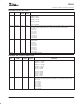
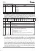
Specifications


SLAS495A− JUNE 2006 − REVISED OCTOBER 2007
www.ti.com
79
With this in mind, power to the TSC2111 should be clean and well bypassed. A 0.1 µF ceramic bypass capacitor
should be placed as close to the device as possible. A 1 µF to 10 µF capacitor may also be needed if the
impedance of the connection between the TSC2111 supply pins and system power supply is high.
A 1 µF bypass capacitor should be placed on the VREF pin if the SAR ADC is intended to be used with the
internal reference voltagel. If an external reference voltage originates from an op amp, make sure that it can
drive any bypass capacitor that is used without oscillation.
The TSC2111 architecture offers no inherent rejection of noise or voltage variation in regards to using an
external reference input. This is of particular concern when the reference input is tied to the power supply. Any
noise and ripple from the supply appears directly in the digital results. While high frequency noise can be filtered
out, voltage variation due to line frequency (50 Hz or 60 Hz) can be difficult to remove.
The ground pins should be connected to a clean ground point. In many cases, this is the analog ground. Avoid
connections, which are too near the grounding point of a microcontroller or digital signal processor. If needed,
run a ground trace directly from the converter to the power supply entry or battery connection point. The ideal
layout includes an analog ground plane dedicated to the converter and associated analog circuitry.
In the specific case of use with a resistive touch screen, care should be taken with the connection between the
converter and the touch screen. Since resistive touch screens have fairly low resistance, the interconnection
should be as short and robust as possible. Loose connections can be a source of error when the contact
resistance changes with flexing or vibrations.
As indicated previously, noise can be a major source of error in touch-screen applications (e.g., applications
that require a back-lit LCD panel). This EMI noise can be coupled through the LCD panel to the touch screen
and cause flickering of the converted ADC data. Several things can be done to reduce this error, such as utilizing
a touch screen with a bottom−side metal layer connected to ground. This couples the majority of noise to
ground. Additionally, filtering capacitors, from Y+, Y–, X+, and X– to ground, can also help. Note, however, that
the use of these capacitors increases screen settling time and require longer panel voltage stabilization times,
as well as increased precharge and sense times for the PINTDAV
circuitry of the TSC2111.