
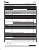
Specifications


SLAS495A− JUNE 2006 − REVISED OCTOBER 2007
www.ti.com
8
ELECTRICAL CHARACTERISTICS (continued)
At +25°C, AVDD1, AVDD2, DRVDD, IOVDD = 3.3 V, BVDD = 3.9 V, DVDD = 1.8 V, V
ref
= 2.5 V, Fs (Audio) = 48 kHz, unless otherwise noted
(continued)
PARAMETER TEST CONDITIONS MIN TYP MAX UNITS
CP_INP TO 32Ω RECEIVER
(SPK1−OUT32N)
1020-Hz Sine wave input on CP_IN, Load on
SPK1−OUT32N = 32 Ω (differential), 50 pF
Full-scale input voltage (0 dB) 0.707 Vrms
Input common mode 1.5 V
Full-scale output voltage (0 dB) 1.697 Vrms
Output common mode 1.5 V
SNR Measured as idle channel noise, A-weighted 97 dBA
THD 0 dBFs input, 0 dB gain −82 dB
CP_IN (Differential) into 32−W
1020-Hz Sine wave input on
CP_INP−CP_INM. Load is connected between
SPK1−OUT32N.
Load = 32 Ω (Differential), 50 pF
Full-scale input voltage (0 dB) 1.414 Vrms
Input common mode 1.5 V
Full-scale output voltage (0 dB) 1.697 Vrms
Output common mode 1.5 V
SNR Measured as idle channel noise, A-weighted 85 101 dBA
THD 0 dBFs input, 0 dB gain −80 −60 dB
PSRR
217 Hz, 100 mV on AVDD1/AVDD2/DRVDD −74
dB
PSRR
1020 Hz, 100 mV on AVDD1/AVDD2/DRVDD −74
dB
Interchannel isolation −85 dB
Mute attenuation 120 dB
Maximum output power 82 mW
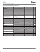
DIGITAL INPUT/OUTPUT
Logic family CMOS
Logic level: V
IH
I
IH
= 5 µA, IOVDD >1.6 V 0.7xIOVDD V
Logic level: V
IH
I
IH
= 5 µA, IOVDD <1.6 V IOVDD V
V
IL
I
IL
= +5 µA, IOVDD <1.6 V −0.3 0.3xIOVDD V
V
IL
I
IL
= +5 µA, IOVDD <1.6 V 0 V
V
OH
I
OH
= 2 TTL loads 0.8IOVDD V
V
OL
I
OL
= 2 TTL loads 0.1IOVDD V
Capacitive load 10 pF