MI953 Intel ® ArrandaleTM /PCH Mini-ITX Motherboard USER’S MANUAL Version 1.
Acknowledgments AMI is a registered trademark of American Megatrends Inc. PS/2 is a trademark of International Business Machines Corporation. Intel and Intel® Arrandale DC Mobile Processor are registered trademarks of Intel Corporation. Microsoft Windows is a registered trademark of Microsoft Corporation. Fintek is a registered trademark of Fintek Electronics Corporation. All other product names or trademarks are properties of their respective owners.
Table of Contents Introduction ....................................................... 1 Product Description ............................................................. 1 Checklist .............................................................................. 2 MI953 Specifications .......................................................... 3 Board Dimensions ............................................................... 4 Installations .......................................................
IMPORTANT NOTE: When the system boots without the CRT being connected, there will be no image on screen when you insert the CRT/VGA cable. To show the image on screen, the hotkey must be pressed (CTRL-ALT-F1).
INTRODUCTION Introduction Product Description The MI953 Mini ITX board incorporates the Intel® Chipset for Embedded Computing, consisting of the Intel® Arrandale DC mobile processor (integrated Graphic and Memory Controller) and Intel® Ibex Peak-M (PCH), an optimized integrated graphics solution with a 800/1066MHz front-side bus. Dimensions of the board are 170mm x 170mm.
INTRODUCTION Checklist Your MI953 package should include the items listed below.
INTRODUCTION MI953 Specifications CPU Supported CPU Voltage System Speed CPU FSB Cache Green /APM CPU Socket Chipset BIOS Memory VGA LVDS LCD Panel LAN USB Serial ATA Ports IAMT6.0 Audio LPC I/O Digital IO Keyboard/Mouse Expansion Slots Edge Connector Onboard Header/ Connector Watchdog Timer System Voltage Others Board Size Intel® Arrandale DC mobile processor 0.700V ~ 1.5V (IMVP-6.5) Up to 3.0GHz or above 1066MHz FSB Up to 4MB shared L3 Cache APM1.
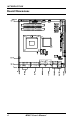
INTRODUCTION [ Board Dimensions 4 MI953 User’s Manual
INTRODUCTION MI953 User’s Manual 5
INSTALLATIONS Installations This section provides information on how to use the jumpers and connectors on the MI953 in order to set up a workable system. The topics covered are: Installing the CPU.................................................................................. 7 Installing the Memory ............................................................................ 8 Setting the Jumpers ................................................................................ 9 Connectors on MI953 ......
INSTALLATIONS Installing the CPU The MI953 board supports rPGA989 socket for Intel® Arrandale Dual Core mobile processors. The processor socket comes with a screw to secure the processor. As shown in the left picture below, loosen the screw first before inserting the processor. Place the processor into the socket by making sure the notch on the corner of the CPU corresponds with the notch on the inside of the socket. Once the processor has slide into the socket, fasten the screw.
INSTALLATIONS Installing the Memory The MI953 board supports two DDR3 memory socket for a maximum total memory of 8GB in DDR3 SO-DIMM memory type. Installing and Removing Memory Modules To install the DDR3 modules, locate the memory slot on the board and perform the following steps: 1. Hold the DDR3 module so that the key of the DDR3 module aligned with that on the memory slot. 2.
INSTALLATIONS Setting the Jumpers Jumpers are used on MI953 to select various settings and features according to your needs and applications. Contact your supplier if you have doubts about the best configuration for your needs. The following lists the connectors on MI953 and their respective functions. Jumper Locations on MI953 ................................................................ 10 JP1: LCD Panel Power Selection ........................................................
INSTALLATIONS Jumper Locations on MI953 Jumpers on MI953 ........................................................................... Page JP1: LCD Panel Power Selection......................................................... 11 JP3, JP4, JP5: RS232/422/485 (COM2) Selection .............................. 11 JP6: PCI/PCIE Riser Card Selection.................................................... 12 JBAT1: Clear CMOS Setting...............................................................
INSTALLATIONS JP1: LCD Panel Power Selection JP1 LCD Panel Power 3.3V 5V JP3, JP4, JP5: RS232/422/485 (COM2) Selection COM1 is fixed for RS-232 use only. COM2 is selectable for RS232, RS-422 and RS-485. The following table describes the jumper settings for COM2 selection.
INSTALLATIONS COM2 is jumper selectable for RS-232, RS-422 and RS-485.
INSTALLATIONS Connectors on MI953 Connector Locations on MI953 ........................................................... 14 CN1: DVI-D and DVI-I Connector ..................................................... 15 CN2, CN3: COM1 and VGA Connector ............................................. 16 CN4: PS/2 Keyboard/Mouse Connectors and USB5/6 Ports .............. 16 USB_LAN1: 10/100/1000 RJ-45 (MI953F) and USB3/4 Ports .......... 17 USB_LAN2: 10/100/1000 RJ-45 (MI953) and USB1/2 Ports ............
INSTALLATIONS Connector Locations on MI953 14 MI953 User’s Manual
INSTALLATIONS CN1: DVI-D and DVI-I Connector [ Signal Name Pin # Pin # Signal Name DATA 2DATA 2+ Shield 2/4 DATA 4DATA 4+ DDC CLOCK DDC DATA N.C DATA 1DATA 1+ SHIELD 1/3 DATA 3DATA 3+ DDC POWER A GROUND 1 1 2 3 4 5 6 7 8 9 10 11 12 13 14 15 16 17 18 19 20 21 22 23 24 C1 C2 C3 C4 C5 C6 HOT POWER DATA 0DATA 0+ SHIELD 0/5 DATA 5DATA 5+ SHIELD CLK CLOCK CLOCK + N.C. N.C. N.C. N.C. N.C. N.C. Signal Name Pin # Pin # Signal Name DATA 2DATA 2+ Shield 2/4 DATA 4DATA 4+ DDC CLOCK DDC DATA N.
INSTALLATIONS CN2, CN3: COM1 and VGA Connector Signal Name Pin # DCD 1 RXD 2 TXD 3 DTR 4 GND 5 [ Pin # Signal Name 6 DSR 7 RTS 8 CTS 9 RI 10 Not Used [[[[ Signal Name Pin # Red Blue GND GND N.C. N.C. HSYNC DDC_CLK 1 3 5 7 9 11 13 15 Pin # Signal Name 2 4 6 8 10 12 14 Green N.C.
INSTALLATIONS USB_LAN1: 10/100/1000 RJ-45 (MI953F) and USB3/4 Ports USB_LAN2: 10/100/1000 RJ-45 (MI953) and USB1/2 Ports CN5: Audio Connector The audio connector, from top to bottom, is composed of Line in, Line out and Microphone jacks.
INSTALLATIONS ATX1: ATX Power Supply Connector 11 1 20 10 Signal Name 3.3V -12V Ground PS-ON Ground Ground Ground -5V +5V +5V Pin # 11 12 13 14 15 16 17 18 19 20 Pin # 1 2 3 4 5 6 7 8 9 10 Signal Name 3.3V 3.3V Ground +5V Ground +5V Ground Power good 5VSB +12V J1 (F_PANEL): System Function Connector J1 provides connectors for system indicators that provide light indication of the computer activities and switches to change the computer status.
INSTALLATIONS Power LED: Pins 11 - 15 Pin # 11 12 13 14 15 Signal Name Power LED No connect Ground No connect Ground ATX Power ON Switch: Pins 7 and 17 This 2-pin connector is an “ATX Power Supply On/Off Switch” on the system that connects to the power switch on the case. When pressed, the power switch will force the system to power on. When pressed again, it will force the system to power off.
INSTALLATIONS F_USB1: USB7/USB8 Connector Signal Name Vcc D0D0+ Ground Pin 1 3 5 7 Pin 2 4 6 8 Signal Name Vcc D1D1+ Ground NC 9 10 Ground Signal Name Vcc D0D0+ Ground Pin 1 3 5 7 Pin 2 4 6 8 Signal Name Vcc D1D1+ Ground NC 9 10 Ground F_USB2: USB9/USB10 Connector COM2: COM2 Serial Port COM2 Signal Name DCD, Data carrier detect RXD, Receive data TXD, Transmit data DTR, Data terminal ready GND, ground 20 Pin # 1 2 3 4 5 Pin # 6 7 8 9 10 Signal Name DSR, Data set ready RTS, Request to
INSTALLATIONS LVDS1, LVDS2: LVDS Connectors (1st channel, 2nd channel) The LVDS connectors on board consist of the first channel (LVDS1) and second channel (LVDS2). Signal Name TX0Ground TX15V/3.3V TX3TX2Ground TXC5V/3.
INSTALLATIONS J5: SPI Flash Connector (factory use only) J6: Front Audio Connector Signal Name Pin # MIC2_L 1 MIC2_R 3 Line2_L 5 Sense 7 Line2_R 9 Pin # 2 4 6 8 10 Signal Name Ground Presence# MIC2_ID NC Line2_ID J7: PCI-E(x1) Slot J8: SPDIF Out Connector PCI1: PCI Slot (supports 2 Master) JMINI: Mini PCIE Connector SATA1, SATA2, SATA3, SATA4: SATA Connectors 22 MI953 User’s Manual
BIOS SETUP BIOS Setup This chapter describes the different settings available in the AMI BIOS that comes with the board. The topics covered in this chapter are as follows: BIOS Introduction ........................................................................................ 24 BIOS Setup .................................................................................................... 24 Main BIOS Setup .........................................................................................
BIOS SETUP BIOS Introduction The BIOS (Basic Input/Output System) installed in your computer system’s ROM supports Intel processors. The BIOS provides critical low-level support for a standard device such as disk drives, serial ports and parallel ports. It also password protection as well as special support for detailed fine-tuning of the chipset controlling the entire system. BIOS Setup The BIOS provides a Setup utility program for specifying the system configurations and settings.
BIOS SETUP Main BIOS Setup This setup allows you to record some basic hardware configurations in your computer system and set the system clock. Aptio Setup Utility Main Advanced Chipset Boot Security BIOS INFORMATION BIOS Vendor Core Version AMI CodeBase Version American Megatrends 4.6.3.7 1ABPZ 0.
BIOS SETUP Advanced Settings This section allows you to configure and improve your system and allows you to set up some system features according to your preference.
BIOS SETUP PCI Subsystem Settings This section allows you to configure the PCI, PCI-X and PCI Express settings. Aptio Setup Utility Main Advanced Chipset Boot Security PCI Bus Driver Version PCI ROM Priority V 2.02.
BIOS SETUP Extended Tag If ENABLED allows Device to use 8-bit Tag field as a requester. No Snoop Enables or Disables PCI Express Device No Snoop option. Maximum Payload Set Maximum Payload of PCI Express Device or allow System BIOS to select the value. Maximum Read Request Launches (Enabled/Disabled) the boot option for legacy network devices. PCI Express Link Settings Set Maximum Read Request Size of PCI Express Device or allow System BIOS to select the value.
BIOS SETUP ACPI Settings Aptio Setup Utility Main Advanced Chipset Boot Security Enable ACPI Auto Configuration Disabled Enable Hibernation ACPI Sleep State Enabled S3 (Suspend to R…) Save & Exit → ← Select Screen ↑↓ Select Item Enter: Select +- Change Field F1: General Help F2: Previous Values F3: Optimized Default F4: Save ESC: Exit Enabled ACPI Auto Configuration Enables or Disables BIOS ACPI Auto Configuration.
BIOS SETUP Wake up event settings Aptio Setup Utility Main Advanced Chipset Boot Wake system with Fixed Time Wake up hour Wake up minute Wake up second Disabled 0 0 0 Wake on Ring Wake on PME Enabled Enabled Security Save & Exit → ← Select Screen ↑↓ Select Item Enter: Select +- Change Field F1: General Help F2: Previous Values F3: Optimized Default F4: Save ESC: Exit Wake system with Fixed Time Enables or Disables System wake on alarm event.
BIOS SETUP CPU Configuration This section shows the CPU configuration parameters.
BIOS SETUP Adjacent Cache Line Prefetch To turn on/off prefetching of adjacent cache lines. Intel Virtualization Technology When enabled, a VMM can utilize the additional hardware capabilities provided by Vanderpool Technology. Power Technology Enable the power management features. TDC Limit / TDP Limit Turbo-XE Mode Processor TDC Limit in 1/8 A granularity. 0 means using the factory-configured value. SATA Configuration SATA Devices Configuration.
BIOS SETUP Thermal Configuration Aptio Setup Utility Main Advanced Chipset Boot Security Save & Exit Thermal Configuration ME SMBus Thermal Reporting PPEC PTL MMGPC MPPC PTA PTA_OFFSET MGTA MGTA_OFFSET 0 0 0 0 128 140 128 140 MCH Temp Read PCH Temp Read CPU Energy Read CPU Temp Read Thermal Data Reporting Enabled Enabled Enabled Enabled Enabled Alert Enable Lock Disabled → ← Select Screen ↑↓ Select Item Enter: Select +- Change Field F1: General Help F2: Previous Values F3: Optimized Default F
BIOS SETUP PTA_OFFSET PCH offset for calculating PCH temperature. MGTA MCH/GfX Temperature Adjust. MGTA_OFFSET MCH/GfX offset for calculating MCH/GfX Temperature. MCH Temp Read MCH Temperature Read Enable. PCH Temp Read PCH Temperature Read Enable. CPU Energy Read CPU Energy Read Enable. CPU Temp Read CPU Temperature Read Enable. Thermal Data Reporting Thermal Data Reporting Enable. Alert Enable Lock Lock all Alert Enable settings.
BIOS SETUP Intel IGD SWSCI OpRegion Aptio Setup Utility Main Advanced Chipset Boot Security Save & Exit Intel IGD SWSCI OpRegion Configuration DVMT/FIXED Memory IGD – Boot Type Active LFP Panel Color Depth LFP LCD Panel Type Panel Scaling Backlight Control BIA Control Spread Spectrum Clock Chip ALS Support Gfx Low Power Mode 256MB VBIOS Default No LVDS 18 Bit 1024 x 768 LVDS Auto PWM Inverted VBIOS Default Off Disabled Enabled → ← Select Screen ↑↓ Select Item Enter: Select +- Change Field F1: Gen
BIOS SETUP Spread Spectrum Clock Chip The default setting is Off. Other options are: Hardware: Spread is controlled by chip. Software: Spread is controlled by BIOS. ALS Support Enabled or Disabled. Valid only for ACPI. Legacy = ALS Support through the IGD INT10 function. ACPI = ALS suport through an ACPI ALS driver. Gfx Low Power Mode Enabled or Disabled. This option is applicable for SFF only.
BIOS SETUP Intel TXT(LT) Configuration Aptio Setup Utility Main Advanced Chipset Boot Security Save & Exit Intel Trusted Execution Technology Configuration → ← Select Intel TXT (LT) Support Disabled Screen ↑↓ Select Item Enter: Select +- Change Field F1: General Help F2: Previous Values F3: Optimized Default F4: Save ESC: Exit Intel TXT (LT) Support Enable/Disable Intel Trusted Execution Technology Support.
BIOS SETUP Super IO Configuration Aptio Setup Utility Main Advanced Chipset Boot Security Save & Exit Super IO Configuration Super IO Chip -> Serial Port 0 Configuration -> Serial Port 1 Configuration -> Serial Port 2 Configuration -> Serial Port 3 Configuration Power Failure Fintek F81865 Always off → ← Select Screen ↑↓ Select Item Enter: Select +- Change Field F1: General Help F2: Previous Values F3: Optimized Default F4: Save ESC: Exit Serial Port Configuration Set Parameters of Serial Ports
BIOS SETUP H/W Monitor Aptio Setup Utility Main Advanced Chipset Boot Security Save & Exit PC Health Status System Temperature1 System Temperature 2 System FAN1 Speed System FAN2 Speed VCC3V Vin0 Vin2 Vin3 VSB3V VBAT Fan1 Smart Fan Control Fan2 Smart Fan Control +51 C +35 C N/A 7109 RPM +3.408 V +0.928 V +5.087 V +12.232 V +3.424 V +3.
BIOS SETUP AMT Configuration Aptio Setup Utility Main Advanced Chipset AMT Unconfigure AMT/ME WatchDog Timer OS WatchDog Timer BIOS WatchDog Timer Boot Security Enabled Disabled Disabled 0 0 Save & Exit → ← Select Screen ↑↓ Select Item Enter: Select +- Change Field F1: General Help F2: Previous Values F3: Optimized Default F4: Save ESC: Exit AMT Options are Enabled and Disabled. Unconfigure AMT/ME Perform AMT/ME unconfigure without password operation.
BIOS SETUP Intel ME Subsystem This section allows you to configure the PCI settings. Aptio Setup Utility Main Advanced Chipset Boot Security Save & Exit Intel ME Subsystem Configuration ME Version 6.0.3.
BIOS SETUP Chipset Settings This section allows you to configure and improve your system and allows you to set up some system features according to your preference. Aptio Setup Utility Main Advanced Enable CSID ► North Bridge ► South Bridge ► ME Subsystem Chipset Boot Security Save & Exit Disabled → ← Select Enable CSID By default, this item is disabled. Enable Compatible Revision ID. North Bridge This item shows the North Bridge Parameters.
BIOS SETUP North Bridge This section allows you to configure the North Bridge Chipset.
BIOS SETUP PCI Express Port Options are Disabled, Enabled and Auto. IGD Memory IGD Share Memory Size. Options are Disable, 32M, 64M and 128M. PAVP Mode Select PAVP Mode used by Internal Graphics Device. Options are Disabled and Enabled. PEG Force Gen1 PCI Express Port Force Gen1.
BIOS SETUP SB Chipset Configuration This section allows you to configure the South Bridge Chipset.
BIOS SETUP PCI Express Ports Configuration Enable or Disable the PCI Express Ports in the Chipset.
BIOS SETUP Boot Settings This section allows you to configure the boot settings according to your preference. Aptio Setup Utility Main Advanced Chipset Boot Boot Configuration Quiet Boot Fast Boot Setup Prompt Timeout Bootup NumLock State CSM16 Module Version GateA20 Active Option ROM Messages Interrupt 19 Canture Boot Option Priorities Boot Option #1 Security Disabled Disabled 1 On 07.
BIOS SETUP Boot Option Priorities Sets the system boot order. Hard Drive BBS Priorities Set the order of the legacy devices in this group. Security Settings This section allows you to configure and improve your system and allows you to set up some system features according to your preference.
BIOS SETUP Save & Exit Settings Aptio Setup Utility Main Advanced Chipset Boot Security Save Changes and Exit Disacard Changes and Exit Save Changes and Reset Discard Changes and Reset Save & Exit → ← Select Screen ↑↓ Select Item Enter: Select +- Change Field F1: General Help F2: Previous Values F3: Optimized Default F4: Save ESC: Exit Save Options Save Changes Discard Changes Restore Defaults Save as User Defaults Restore User Defaults Boot Override SATA: ATAPI iHDS116 4 SATA: Hitachi HDS721616P
BIOS SETUP Save as User Defaults Save the changes done so far as User Defaults. Restore User Defaults Restore the User Defaults to all the setup options. Boot Override Pressing ENTER causes the system to enter the OS. Launch EFI Shell from filesystem device Attempts to Launch EFI Shell application (Shellx64.efi) from one of the available filesystem devices. Reset System with ME disable Mode ME will run into the temporary disable mode.
DRIVERS INSTALLATION Drivers Installation This section describes the installation procedures for software and drivers under the Windows 2000 and Windows XP. The software and drivers are included with the motherboard. If you find the items missing, please contact the vendor where you made the purchase. The contents of this section include the following: Intel Chipset Software Installation Utility ........................................... 52 VGA Drivers Installation ........................................
DRIVER INSTALLATION Intel Chipset Software Installation Utility The Intel Chipset Drivers should be installed first before the software drivers to enable Plug & Play INF support for Intel chipset components. Follow the instructions below to complete the installation. 1. Insert the CD that comes with the board. Click Intel and then Intel(R) QM57 Chipset Drivers. 2. Click Intel(R) Chipset Software Installation Utility. 3.
DRIVERS INSTALLATION 4. Click Yes to accept the software license agreement and proceed with the installation process. 5. On the Readme File Information screen, click Next to continue the installation. 6. The Setup process is now complete. Click Finish to restart the computer and for changes to take effect.
DRIVER INSTALLATION VGA Drivers Installation NOTE: Before installing the Intel(R) QM57 Chipset Family Graphics Driver, the Microsoft .NET Framework 3.5 SPI should be first installed. To install the VGA drivers, follow the steps below. 1. Insert the CD that comes with the board. Click Intel and then Intel(R) QM57 Chipset Drivers. 2. Click Intel(R) QM57 Chipset Family Graphics Driver. 3. When the Welcome screen appears, click Next to continue.
DRIVERS INSTALLATION 4. Click Yes to to agree with the license agreement and continue the installation. 5. On the Readme File Information screen, click Next to continue the installation of the Intel® Graphics Media Accelerator Driver. 6. On Setup Progress screen, click Next to continue. 7. Setup complete. Click Finish to restart the computer and for changes to take effect.
DRIVER INSTALLATION Realtek HD Audio Driver Installation Follow the steps below to install the Realtek HD Audio Drivers. 1. Insert the CD that comes with the board. Click Intel and then Intel(R) QM57 Chipset Drivers. 2. Click Realtek High Definition Audio Driver. 3. On the Welcome to the InstallShield Wizard screen, click Next. 3. InstallShield Wizard is complete. Click Finish to restart the computer.
DRIVERS INSTALLATION LAN Drivers Installation Follow the steps below to install the Intel LAN drivers. 1. Insert the CD that comes with the board. Click Intel and then Intel(R) QM57 Chipset Drivers. 2. Click Intel(R) PRO LAN Network Driver. 3. When the Welcome screen appears, click Next. On the next screen, click Yes to to agree with the license agreement.
DRIVER INSTALLATION 4. Click the checkbox for Drivers in the Setup Options screen to select it and click Next to continue. 5. The wizard is ready to begin installation. Click Install to begin the installation.
DRIVERS INSTALLATION 6. When InstallShield Wizard is complete, click Finish.
DRIVER INSTALLATION Intel® Management Engine Interface NOTE: Before installing the Intel(R) AMT 6.0 Drivers, the Microsoft .NET Framework 3.5 SPI should be first installed. Follow the steps below to install the Intel Management Engine. 1. Insert the drivers disc that comes with the motherboard. Click Intel and then Intel(R) AMT 6.0 Drivers.
DRIVERS INSTALLATION 2. When the Welcome screen to the InstallShield Wizard for Intel® Management Engine Components, click Next. On the next screen, click Yes to to agree with the license agreement. 2. When the Setup Progress screen appears, click Next. Then, click Finish when the setup progress has been successfully installed.
DRIVER INSTALLATION 62 MI953 User’s Manual
APPENDIX Appendix A. I/O Port Address Map Each peripheral device in the system is assigned a set of I/O port addresses which also becomes the identity of the device. The following table lists the I/O port addresses used.
APPENDIX B. Interrupt Request Lines (IRQ) Peripheral devices use interrupt request lines to notify CPU for the service required. The following table shows the IRQ used by the devices on board.
APPENDIX C. Watchdog Timer Configuration The WDT is used to generate a variety of output signals after a user programmable count. The WDT is suitable for use in the prevention of system lock-up, such as when software becomes trapped in a deadlock. Under these sorts of circumstances, the timer will count to zero and the selected outputs will be driven. Under normal circumstance, the user will restart the WDT at regular intervals before the timer counts to zero.
APPENDIX //--------------------------------------------------------------------------void EnableWDT(int interval) { unsigned char bBuf; bBuf = Get_F81865_Reg(0x2B); bBuf &= (~0x20); Set_F81865_Reg(0x2B, bBuf); //Enable WDTO Set_F81865_LD(0x07); Set_F81865_Reg(0x30, 0x01); //switch to logic device 7 //enable timer bBuf = Get_F81865_Reg(0xF5); bBuf &= (~0x0F); bBuf |= 0x52; Set_F81865_Reg(0xF5, bBuf); //count mode is second Set_F81865_Reg(0xF6, interval); //set timer bBuf = Get_F81865_Reg(0xFA); bBuf
APPENDIX //--------------------------------------------------------------------------// // THIS CODE AND INFORMATION IS PROVIDED "AS IS" WITHOUT WARRANTY OF ANY // KIND, EITHER EXPRESSED OR IMPLIED, INCLUDING BUT NOT LIMITED TO THE // IMPLIED WARRANTIES OF MERCHANTABILITY AND/OR FITNESS FOR A PARTICULAR // PURPOSE. // //--------------------------------------------------------------------------#include "F81865.H" #include
APPENDIX outportb(F81865_INDEX_PORT, REG); Result = inportb(F81865_DATA_PORT); Lock_F81865(); return Result; } //--------------------------------------------------------------------------- //--------------------------------------------------------------------------// // THIS CODE AND INFORMATION IS PROVIDED "AS IS" WITHOUT WARRANTY OF ANY // KIND, EITHER EXPRESSED OR IMPLIED, INCLUDING BUT NOT LIMITED TO THE // IMPLIED WARRANTIES OF MERCHANTABILITY AND/OR FITNESS FOR A PARTICULAR // PURPOSE.