AMN11310 TM WHDI Transmitter Module Datasheet Version 0.4 Version 0.
Important Notice Important Notice AMIMON Ltd. reserves the right to make corrections, modifications, enhancements, improvements, and other changes to its products and services at any time and to discontinue any product or service without notice. Customers should obtain the latest relevant information before placing orders and should verify that such information is current and complete. All products are sold subject to AMIMON's terms and conditions of sale supplied at the time of order acknowledgment.
Revision History Revision History Version Date Description 0.1 - Initial Release 0.2 15.6.08 Revision of RFIC board revB 0.3 0.4 20.7.08 2.9.08 Board Mechanical size Reset and Wake-up Timer modified RF frame modified Power switch on RF removed Operating Conditions and Electrical Characteristics modified AMN11310 Block Diagram modified Unhide Certification & Compliance Power requirements Mini-MAC changed to MAC Add chapter RF AMN3110 Antenna diversity.
Table of Contents Table of Contents List of Figures......................................................................................................................................................... vi List of Tables .......................................................................................................................................................... vi Chapter 1, Introduction .............................................................................................. 1 1.
Table of Contents Chapter 5, Electrical Specifications ........................................................................ 21 5.1 5.2 Operating Conditions and Electrical Characteristics ............................................................................. 21 RF Characteristics TBD ............................................................................................................................. 22 Chapter 6, Design Guidelines ........................................................
List of Figures List of Figures Figure 1: AMN11310 Block Diagram......................................................................................................................... 3 Figure 2: WHDI Baseband Transmitter Chipset ........................................................................................................ 4 Figure 3: Video Data Processing Path ......................................................................................................................
Introduction Chapter 1 Introduction TM The AMN11310 is the second generation of WHDI transmitter board. It is based on AMIMON's WHDI transmitter chipset: the AMN2110 baseband transmitter and the AMN3110 RFIC transmitter. TM The AMN11310 WHDI wireless transmitter module, together with the AMN12310 wireless receiver module, presents the ultimate solution for converting any High Definition (HD) system into a wireless one.
Introduction • • RF characteristics: MIMO technology, using 5GHz unlicensed band, 18MHz bandwidth. Coexists with 802.11a/n and 5.8GHz cordless devices. Support for Automatic Transmission Power Control (ATPC). No line of sight needed between transmitter and receiver. It has a range of over 30 meters, suitable for almost any room. 14mW typical transmission power per transmitting channel. Maximum 20mW transmission power per transmitting channel.
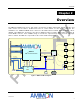
Overview Chapter 2 Overview The AMN11310 WHDI Video Source Unit (VSU) is designed to modulate and transmit downstream video and audio content over the wireless medium and receive a control channel over the wireless upstream. The modulation uses 18MHz bandwidth and is carried over the 5GHz unlicensed band. Figure 1 displays a block diagram of the AMN11310. The inputs to the VSU are digital uncompressed video, digital audio and control, all via the WHDI connector.
Overview The main building blocks of the AMN11310 are as follows: • AMN2110 WHDI Baseband Transmitter, as briefly described on page 4. • STM32F MAC µController, as briefly described on page 4. • AMN3110 WHDI • Power Amplifier (PA), as briefly described on page 5. • Board Connector (WHDI • 40MHz Crystal Oscillator, as described on page 5. • RF AMN3110 Antenna Switching Switch, as described on page 6. 2.1 TM 5GHz Transceiver, as briefly described on page 5.
Overview 2.3 AMN3110 WHDITM 5GHz Transceiver The VSU uses the AMN3110 chip. The AMN3110 is a fully integrated direct conversion MIMO transmitter specifically designed for WHDI applications using OFDM modulation in single-band 4.9GHz to 5.9GHz.
Overview 2.7 RF AMN3110 Antenna Switching Switch The antenna switching switch controls two input options: reception from on board printed antenna or SPIFA (standing antenna) for uplink channel. This switch is controlled by two general purpose pins of the STM32F UC: GPIO PB6 pin#58 and PB7 pin#59. Version 0.
Interfaces Chapter 3 Interfaces 3.1 Video Data Input and Conversions Figure 3: Video Data Processing Path Figure 3 shows the stages for processing video data through the AMN2110. The HSYNC and the VSYNC input signals are mandatory. The DE input signal is optional and can be created with the DE generator using the HSYNC and the VSYNC pulses. The video input data is uncompressed digital video up to 3*10 bits in width. Important: When connected to a 3*8 bits source, connect the appropriate LSBs to GND.
Interfaces Color Space Converter The AMN11310 can receive either RGB or YCbCr color space. For more details, you may refer to the MAC registers in the programmer's reference guide. Common Video Input Format Table 1 describes the common supported video input resolutions. Table 1: Common Supported Video Input Resolutions Color Space Video Format RGB/YCbCr 3.1.1 4:4:4 Input Pixel Clock (MHz) Bus Width 24 480i 27 480p XGA 27 65 720p 1080i 74.25 74.
Interfaces EDGE = 0 EDGE = 1 3.1.2.2 Timing Diagram Figure 4: Timing Diagram 3.2 Audio Data Capture AMN11310 transports an explicit audio master clock with appropriate data-over-the-wireless link. No constraints exist for a coherent video and audio clock, where coherent means that the audio and the video clock must have been created from the same clock source. The AMN11310 can accept digital audio from either SPDIF or I2S inputs.
Interfaces 3.2.1 I2S Bus Specification 2 The AMN11310 supports a standardized communication structure inter-IC sound (I S) bus. As shown in Figure 5, the bus has three lines: continuous serial clock (SCK), word select (WS) and serial data (SD). The external device generating SCK and WS is the audio source. 2 Figure 5: I S Simple System Configurations and Basic Interface Timing 2 The AMN11310 supports an I S format of up to 32 bits for each channel (left and right).
Interfaces 3.2.1.2 Timing Diagram TSCKCYC T SCKDUTY SCK 50% TDCKSETUP TDCKHOLD SD ,WS 2 Figure 6: I S Input Timings 3.2.2 S/PDIF Bus 3.2.2.1 Timing Requirements The AMN11310 does not require the SPDIF clock. The clock is produced internally by sampling the SPDIF data input at a high clock rate and processing it. Table 5: Audio Interface Timing Requirements Symbol Parameter Condition MIN TYP MAX Units TSPCYC SPDIF data sampling rate 162 488 ns TSPFREQ SPDIF data sampling freq 2.
Interfaces 3.3 Management Buses and Connectors 3.3.1 Two-Wire Serial Bus Interface The WHDI application observes and controls the AMN11310 via a Two-Wire interface and an interrupt line connecting the application microcontroller and the AMN11310 MAC microcontroller. The protocol of the Two-Wire bus for the WHDI application/MAC interface is described in the following sections.
Interfaces 3.3.1.3 MAC uC Write Operation Figure 8 demonstrates a write transaction which sends 2 data bytes and which ends with the master stop bit. Each write transaction sends 1 or more data bytes to the MAC, beginning at an explicit 2 bytes long address. Multiple data bytes may be written as the MAC stores the received register data until the master sends a stop bit. The MAC updates the register value upon a successful termination of a write transaction. Two-Wire Slave address START I6 I5 ...
Interfaces 3.3.3 WHDI Module Configuration In order to distinguish between boards and by the SW, there is an on board id that can be read by the STM32F. WHDI_MODULE_ID (Details) Amimon Project Part Number Tx="0", Interrupt Polarity: I2C Address: "00"=0x62, Rx="1" "0"=falling, "1"=rising "01"=0x72, 10"=0x60, 11"=0x70 MODULE_ID [7] [6] [5] [4] [3] [2] [1] [0] AMN11310 Rev. 2.0 1 0 0 0 0 0 0 0 AMN12310 Rev. 2.0 1 0 1 0 0 0 1 0 3.
Interfaces The following table specifies the timing parameters Table 7: Reset Timing Requirements Symbol Parameter Condition MIN TYP MAX Units TRST-CLK Time from assertion of the HW reset until valid clock is generated 40 MHz clock is valid – few us after power up 300 ns TST,RST Time from assertion of the HW reset until the STM32F completes the internal initialization Power is stable 4.
Interfaces Version 0.
WHDI Connector Pins Chapter 4 WHDI Connector Pins 4.
WHDI Connector Pins 4.2 Connector Schematics Figure 12: WHDI Connector Version 0.
WHDI Connector Pins 4.3 Pin List Table 9: Tx WHDI Connector Pin List Pin Number Signal Pin Number Signal Pin Number Signal Pin Number Signal 1 3.3V 2 3.3V 41 WHDI_D26 42 WHDI_D27 3 3.3V 4 3.3V 43 WHDI_D24 44 WHDI_D25 5 3.3V 6 3.3V 45 WHDI_D22 46 WHDI_D23 7 3.3V 8 3.3V 47 WHDI_D20 48 WHDI_D21 9 3.3V 10 3.3V 49 WHDI_D18 50 WHDI_D19 11 3.3V 12 3.3V 51 WHDI_D16 52 WHDI_D17 13 3.3V 14 3.
WHDI Connector Pins Version 0.
Electrical Specifications Chapter 5 Electrical Specifications 5.1 Operating Conditions and Electrical Characteristics The following tables describe the operating conditions and electrical characteristics required for working with the AMN11310. Table 10: Absolute Maximum Ratings over Operating Case Temperature Range Supply input-voltage range, VI 0 to 3.6 V Ambient temperature range 0°C to 70°C Storage temperature range, Tstg -40°C to 125°C Table 11: Recommended Operating Conditions Parameter Min.
Electrical Specifications 5.2 RF Characteristics (TBD) Version 0.
Design Guidelines Chapter 6 Design Guidelines 6.1 Digital Layout Recommendation To better understand the layout guidelines, please refer to the AMN11310 schematics which are part of the HDK package. 6.1.1 Stack up Recommended stack up for six layers design: • Total thickness: 1.15mm • Tolerance thickness: 10% Table 13: Digital Layout Recommendation Lay. No. 1 Layer Name Component side (CS) Layer Stackup 1-1.
Design Guidelines 6.1.2 General Guidelines • Keep traces as short as possible. • Traces should be routed over full solid reference plans. • Sensitive lines like reset and clocks should be routed with special care. • These lines should be routed over full solid power plans (ground or power). Traces should be routed at least 2 times the trace width away from other lines in the same routing layer. Place a series resistor ~30 ohm at the clock source.
Design Guidelines 6.3 Test Points and Jumpers Table 14 test points and jumpers Reference Name Type Functionality Reference Name Type Functionality TP1 SMD RSSI_DETECT TP29 SMD 3.3V TP2 SMD RFSPI_ODUT TP30 SMD 3.3V TP3 SMD RFSPI_CS TP31 SMD 3.3V TP4 SMD RFSPI_CLK TP32 SMD GND TP5 SMD LD_0 TP33 SMD GND TP6 SMD GND TP34 SMD ALBATROSS_TDO TP7 TH GND TP35 SMD GND TP8 SMD GND TP36 SMD HW_ID_1 TP9 TH 1.2V TP37 SMD 3.
Design Guidelines Version 0.
Mechanical Dimensions Chapter 7 Mechanical Dimensions The following shows the mechanical dimensions for the AMN11310: Figure 13: Mechanical Dimensions Top View Version 0.
Mechanical Dimensions Figure 14: Mechanical Dimensions Bottom View Version 0.
Mechanical Dimensions 7.1 RF Shield Frame and Cover Figure 15: RF-Shield Frame Version 0.
Mechanical Dimensions Figure 16: RF-Shield Cover Version 0.