
User Manual


Phone: +1 408 213-9530 | Fax: 408-213-9533 | E-mail: info@ampedrftech.com
Address : 1879 Lundy Ave, ste. 138, San Jose, CA 95131
电话:+86 022-83945100 | 传真:+86 022-83945100 转 111 | E-mail: infocn@ampedrftech.com
地址:天津市华苑产业区海泰西路 18 号西 3B-202(300384)
3
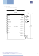
Table of Contents
1 Software Architecture................................................................................................................................................ 4
1.1 Lower Layer Stack ..................................................................................................................................................... 4
1.2 Upper Layer Stack: Amp’ed UP Lite .......................................................................................................................... 4
1.3 HCI Interface .............................................................................................................................................................. 4
1.4 AT Command Set: abSerial ....................................................................................................................................... 4
2 Hardware Specifications ........................................................................................................................................... 5
2.1 Recommended Operating Conditions ........................................................................................................................ 5
2.2 Absolute Maximum Ratings ....................................................................................................................................... 5
2.3 Current Consumption ................................................................................................................................................. 5
2.4 Selected RF Characteristics....................................................................................................................................... 5
Basic Data Rate .................................................................................................................................................................. 5
2.5 I/O Operating Characteristics..................................................................................................................................... 6
2.6 Pin Assignment .......................................................................................................................................................... 7
2.7 Layout Drawing .......................................................................................................................................................... 8
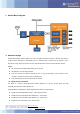
3 Module Block Diagram .............................................................................................................................................. 9
4 Hardware Design ...................................................................................................................................................... 9
4.1 Module Reflow Installation ......................................................................................................................................... 9
4.2 GPIO Interface ......................................................................................................................................................... 10
4.3 UART Interface ........................................................................................................................................................ 10
4.4 PCB Layout Guidelines ............................................................................................................................................ 11
4.5 Reset Circuit............................................................................................................................................................. 11
4.5.1 External Reset Circuit: ........................................................................................................................................... 11
4.5.2 Internal Reset Circuit: ............................................................................................................................................ 12
4.6 External LPO Input Circuit ...................................................................................................................................... 12
4.7 Audio application Reference Design....................................................................................................................... 13
Part 1. WM8904 ................................................................................................................................................................ 13
Part 2. BT Module ............................................................................................................................................................. 13
Part 3. Stereo DAC with Power Amp ................................................................................................................................ 14
5 Regulatory Compliance........................................................................................................................................... 15
5.1 Modular Approval, FCC and IC ................................................................................................................................ 15
5.2 FCC Label Instructions............................................................................................................................................. 15
6 Ordering Information ............................................................................................................................................... 16
7 Revision History ...................................................................................................................................................... 17