
Instruction manual

AMPDIO DRIVERS
Page 68
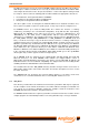
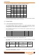
BIT ASSIGNMENTS
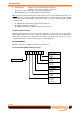
The bit layout of the PPI-X port C data register is shown below.
7 6 5 4 3 2 1 0
PPI-X Port C
Upper Nybble
Data Bits
SK1 44
SK1 5
SK1 63
SK1 24
SK1 4
SK1 62
SK1 23
SK1 42
Digital I/O SK1
Pin Connections
PC4
PC5
PC6
PC7
PPI-X Port C
Lower Nybble
Data Bits
PC0
PC1
PC2
PC3
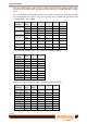
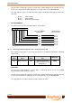
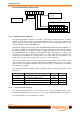
5.4.1.4 82C55 Programmable Peripheral Interface PPI Command Register
This is the command register for the PPI and can be used to set the operational mode of the three
digital I/O ports or to manipulate the bits of port C.
Register
Offset
Write and/or
Read
Register
Width
Register
Title
Mnemonic
03
16
Write 8 bits
82C55 Programmable
Peripheral Interface PPI
Command Register
PPI CMD
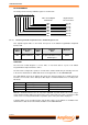
FUNCTION
Provides a command word to define the operation of the PPI ports A, B and C. Any port
programmed as output is initialized to all zeroes when a command word is written. A separate
feature allows any bit of port C to be set or reset using a single instruction.
The programming procedure for the 82C55 is flexible, but the command word must be written
before data bytes are loaded. As the command register and each port have separate addresses
(offsets 0 to 3) and each command word specifies the mode of each port, no other special
instruction sequence is required.
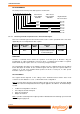
The Three Modes
The register function depends on the setting of bit 7 'Command Select' and the three mode
selections assume that bit 7 is set to '1', which allows mode configuration.
Mode 0 provides basic input and output operations through each of the ports A, B and C. Output
data bits are latched and input data follows the signals applied to the I/O lines. No handshaking is
needed.
16 different configurations in mode 0
Two 8 bit ports and two 4 bit ports
Inputs are not latched
Outputs are latched
Mode 1 provides strobed input and output operations with data transferred through port A or B and
handshaking through port C.