
Specifications


Model 75A250A Manual Text
4-5
REV A
4.3.5 Voltage/Amplifier Faults (Schematic Diagram Nos. 1011806)
The model 75A250A fault circuits sense voltage faults from PS1 (28V). They also sense an over
current fault in the final amplifier stage.
4.3.5.1 Power Supply Faults (Schematic Diagram 1011806). PS1 sends a BUSS OK signal to
the operate/control board (A4). This signal gives an early indication of over voltage or
over current conditions. If either condition occurs the power supply sends a fault signal to
the operate/control board which in turn sends a disable signal to the power supply turning
off the outputs.
4.3.5.2 The Final Amplifier Assy Faults. (Schematic Diagram 1007872 and 1011806). The final
amplifier incorporates two stage protection for the output transistors. U1 monitors the
device current which is normally 6.0 amps. If the amplifier is over driven so that the
current rises to 8.0 amps U1 will decrease the bias voltage thereby decreasing the
current. If the amplifier is over driven to the point that the active bias cannot control the
current to less than 9.0 amps U4 will generate a fault signal which will turn the power
supplies off.
4.3.6 Low or No Power Output (DC Tests) (Schematic Diagram No. 1011806)
All indicators on the Model 75A250A VFD are normal, the VFD indicates “POWER ON” and
“STATUS OK,” and the cooling fan (Blower B1) is operating.
4.3.6.1 Check the RF input to the unit—is it the correct amplitude and frequency?
4.3.6.2 Check the RF output connection from the unit—is it correctly connected to the load?
Is the coaxial cable okay?
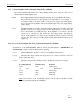
4.3.6.3 Check the voltages at the following locations. Troubleshoot any incorrect voltages.
Feed-through Cap. Normal Voltage Remarks
A3 C9 +12V Gain Control
A3 C12 -12V Gain Control
A1 C1 +28V Driver Stage
A2 C1 +28V Final Amp
A2 C2 +28V Final Amp
Note: The locations of the feed-through capacitors can be found on the RF Assembly
Drawing (Schematic Diagram No. 1010613).