
Datasheet


AD1580
Rev. F | Page 6 of 12
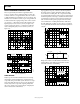
THEORY OF OPERATION
The AD1580 uses the band gap concept to produce a stable,
low temperature coefficient voltage reference suitable for high
accuracy data acquisition components and systems. The device
makes use of the underlying physical nature of a silicon tran-
sistor base emitter voltage in the forward biased operating
region. All such transistors have an approximately −2 mV/°C
temperature coefficient (TC), which is unsuitable for use
directly as a low TC reference; however, extrapolation of
the temperature characteristic of any one of these devices to
absolute zero (with collector current proportional to absolute
temperature) reveals that its V
BE
goes to approximately the
silicon band gap voltage. Thus, if a voltage could be developed
with an opposing temperature coefficient to sum with V
BE
, a
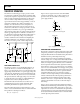
zero TC reference would result. The AD1580 circuit in Figure 10
provides such a compensating voltage, V1, by driving two
transistors at different current densities and amplifying the
resultant V
BE
difference (∆V
BE
, which has a positive TC).
The sum of V
BE
and V1 provides a stable voltage reference.
V+
V–
V1
ΔV
BE
V
BE
00700-010
Figure 10. Schematic Diagram
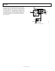
APPLYING THE AD1580
The AD1580 is simple to use in virtually all applications. To
operate the AD1580 as a conventional shunt regulator (see
Figure 11), an external series resistor is connected between the
supply voltage and the AD1580. For a given supply voltage, the
series resistor, R
S
, determines the reverse current flowing through
the AD1580. The value of R
S
must be chosen to accommodate
the expected variations of the supply voltage, V
S
; load current,
I
L
; and the AD1580 reverse voltage, V
R
; while maintaining an
acceptable reverse current, I
R
, through the AD1580.
The minimum value for R
S
should be chosen when V
S
is at
its minimum and I
L
and V
R
are at their maximum, while
maintaining the minimum acceptable reverse current.
The value of R
S
should be large enough to limit I
R
to 10 mA
when V
S
is at its maximum and I
L
and V
R
are at their minimum.
The equation for selecting R
S
is as follows:
R
S
= (V
S
− V
R
)/(I
R
+ I
L
)
Figure 12 shows a typical connection of the AD1580BRT
operating at a minimum of 100 µA. This connection can
provide ±1 mA to the load while accommodating ±10%
power supply variations.
V
S
I
R
+ I
L
R
S
V
OUT
I
L
V
R
I
R
00700-011
Figure 11. Typical Connection Diagram
+5V(+3V) ±10%
2.94kΩ
(1.30kΩ)
R
S
V
R
V
OUT
00700-012
Figure 12. Typical Connection Diagram
TEMPERATURE PERFORMANCE
The AD1580 is designed for reference applications where stable
temperature performance is important. Extensive temperature
testing and characterization ensure that the device’s performance is
maintained over the specified temperature range.
Some confusion exists in the area of defining and specifying
reference voltage error over temperature. Historically, references
have been characterized using a maximum deviation per degree
Celsius, for example, 50 ppm/°C. However, because of nonlinear-
ities in temperature characteristics that originated in standard
Zener references (such as S type characteristics), most manufac-
turers now use a maximum limit error band approach to specify
devices. This technique involves the measurement of the output
at three or more different temperatures to guarantee that the
voltage falls within the given error band. The proprietary
curvature correction design techniques used to minimize the
AD1580 nonlinearities allow the temperature performance to
be guaranteed using the maximum deviation method. This
method is of more use to a designer than the one that simply
guarantees the maximum error band over the entire temper-
ature change.
Figure 13 shows a typical output voltage drift for the AD1580
and illustrates the methodology. The maximum slope of the two
diagonals drawn from the initial output value at +25°C to the
output values at +85°C and −40°C determines the performance
grade of the device. For a given grade of the AD1580, the designer
can easily determine the maximum total error from the initial
tolerance plus temperature variation.