
Datasheet
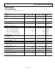


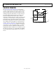
Table Of Contents

AD1582/AD1583/AD1584/AD1585 Data Sheet
Rev. J | Page 10 of 16
THEORY OF OPERATION
The AD1582/AD1583/AD1584/AD1585 use the band gap
concept to produce stable, low temperature coefficient voltage
references suitable for high accuracy data acquisition compo-
nents and systems. These parts of precision references use the
underlying temperature characteristics of a silicon transistor’s
base emitter voltage in the forward-biased operating region.
Under this condition, all such transistors have a −2 mV/°C
temperature coefficient (TC) and a V
BE
that, when extrapolated
to absolute zero, 0 K (with collector current proportional to
absolute temperature), approximates the silicon band gap voltage.
By summing a voltage that has an equal and opposite tempera-
ture coefficient of 2 mV/°C with the V
BE
of a forward-biased
transistor, an almost 0 TC reference can be developed. In the
AD1582/AD1583/AD1584/AD1585 simplified circuit diagram
shown in Figure 9, such a compensating voltage, V1, is derived
by driving two transistors at different current densities and
amplifying the resultant V
BE
difference (∆V
BE
, which has a positive
TC). The sum of V
BE
and V1 (V
BG
) is then buffered and amplified
to produce stable reference voltage outputs of 2.5 V, 3 V, 4.096 V,
and 5 V.
R
4
R6
R5
GN
D
V1
+
–
R3
+
R
2
–
R
1
V
I
N
V
OU
T
V
BG
V
B
E
00701-009
Figure 9. Simplified Schematic