
Datasheet


AD1674
REV. C
–6–
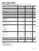
ORDERING GUIDE
INL S/(N+D) Package Package
Model
1
Temperature Range (T
MIN
to T
MAX
)(T
MIN
to T
MAX
) Description Option
2
AD1674JN 0°C to +70°C ±1 LSB 69 dB Plastic DIP N-28
AD1674KN 0°C to +70°C ±1/2 LSB 70 dB Plastic DIP N-28
AD1674JR 0°C to +70°C ±1 LSB 69 dB Plastic SOIC R-28
AD1674KR 0°C to +70°C ±1/2 LSB 70 dB Plastic SOIC R-28
AD1674AR –40°C to +85°C ±1 LSB 69 dB Plastic SOIC R-28
AD1674BR –40°C to +85°C ±1/2 LSB 70 dB Plastic SOIC R-28
AD1674AD –40°C to +85°C ±1 LSB 69 dB Ceramic DIP D-28
AD1674BD –40°C to +85°C ±1/2 LSB 70 dB Ceramic DIP D-28
AD1674TD –55°C to +125°C ±1 LSB 70 dB Ceramic DIP D-28
NOTES
1
For details on grade and package offerings screened in accordance with MIL-STD-883, refer to the Analog Devices Military Products Databook or current
AD1674/883B data sheet. SMD is also available.
2
N = Plastic DIP; D = Hermetic Ceramic DIP; R = Plastic SOIC.
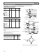
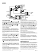
TIMING—STAND-ALONE MODE (Figures 4a and 4b)
J, K, A, B Grades T Grade
Parameter Symbol Min Typ Max Min Typ Max Units
Data Access Time t
DDR
150 150 ns
Low R/
C Pulse Width t
HRL
50 50 ns
STS Delay from R/
C t
DS
200 225 ns
Data Valid After R/
C Low t
HDR
25 25 ns
STS Delay After Data Valid t
HS
0.6 0.8 1.2 0.6 0.8 1.2 µs
High R/C Pulse Width t
HRH
150 150 ns
NOTE
All min and max specifications are guaranteed.
Specifications subject to change without notice.
WARNING!
ESD SENSITIVE DEVICE
CAUTION
ESD (electrostatic discharge) sensitive device. Electrostatic charges as high as 4000 V readily
accumulate on the human body and test equipment and can discharge without detection. Although
the AD1674 features proprietary ESD protection circuitry, permanent damage may occur on
devices subjected to high energy electrostatic discharges. Therefore, proper ESD precautions are
recommended to avoid performance degradation or loss of functionality.
DATA
VALID
DATA VALID
HIGH-Z
STS
DB11 – DB0
R/C
_
t
HRL
t
DS
t
C
t
HS
t
HDR
Figure 4a. Stand-Alone Mode Timing Low Pulse for R/
C
DATA
VALID
HIGH-Z
HIGH-Z
STS
DB11 – DB0
R/C
_
t
HRH
t
DS
t
C
t
DDR
t
HDR
t
HL
Figure 4b. Stand-Alone Mode Timing High Pulse for R/
C
ABSOLUTE MAXIMUM RATINGS*
V
CC
to Digital Common . . . . . . . . . . . . . . . . . . . 0 to + 16.5 V
V
EE
to Digital Common . . . . . . . . . . . . . . . . . . . . . 0 to –16.5 V
V
LOGIC
to Digital Common . . . . . . . . . . . . . . . . . . 0 V to +7 V
Analog Common to Digital Common . . . . . . . . . . . . . . . ±1 V
Digital Inputs to Digital Common . . . –0.5 V to V
LOGIC
+0.5 V
Analog Inputs to Analog Common . . . . . . . . . . . . V
EE
to V
CC
20 V
IN
to Analog Common . . . . . . . . . . . . . . . . . V
EE
to +24 V
REF OUT . . . . . . . . . . . . . . . . . Indefinite Short to Common
. . . . . . . . . . . . . . . . . . . . . . . . . . . Momentary Short to V
CC
Junction Temperature . . . . . . . . . . . . . . . . . . . . . . . . . +175°C
Power Dissipation . . . . . . . . . . . . . . . . . . . . . . . . . . . .825 mW
Lead Temperature, Soldering (10 sec) . . . . . . . +300°C, 10 sec
Storage Temperature . . . . . . . . . . . . . . . . . . .–65°C to +150°C
*Stresses above those listed under “Absolute Maximum Ratings” may cause
permanent damage to the device. This is a stress rating only and functional
operation of the device at these or any other conditions above those indicated in the
operational section of this specification is not implied. Exposure to absolute
maximum rating conditions for extended periods may affect device reliability.