
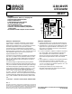
Datasheet
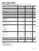


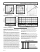

AMPLITUDE – dB
INPUT FREQUENCY – kHz
10000
–100
–120
101
–60
–80
–40
–20
0
1000
THD
2
ND
HARMONIC
3
RD
HARMONIC
f
SAMPLE
= 100kSPS
FULL-SCALE = +10V
100
Figure 5. Harmonic Distortion vs.
Input Frequency
Typical Dynamic Performance–AD1674
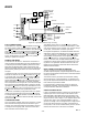
GENERAL CIRCUIT OPERATION
The AD1674 is a complete 12-bit, 10 µs sampling analog-to-
digital converter. A block diagram of the AD1674 is shown on
page 7.
When the control section is commanded to initiate a conversion
(as described later), it places the sample-and-hold amplifier
(SHA) in the hold mode, enables the clock, and resets the suc-
cessive approximation register (SAR). Once a conversion cycle
has begun, it cannot be stopped or restarted and data is not
available from the output buffers. The SAR, timed by the inter-
nal clock, will sequence through the conversion cycle and return
an end-of-convert flag to the control section when the conver-
sion has been completed. The control section will then disable
the clock, switch the SHA to sample mode, and delay the STS
LOW going edge to allow for acquisition to 12-bit accuracy.
The control section will allow data read functions by external
command anytime during the SHA acquisition interval.
During the conversion cycle, the internal 12-bit, 1 mA full-scale
current output DAC is sequenced by the SAR from the most
significant bit (MSB) to the least significant bit (LSB) to pro-
vide an output that accurately balances the current through the
5 kΩ resistor from the input signal voltage held by the SHA.
The SHA’s input scaling resistors divide the input voltage by 2
for the 10 V input span and by 4 V for the 20 V input span,
maintaining a 1 mA full-scale output current through the 5 kΩ
resistor for both ranges. The comparator determines whether
the addition of each successively weighted bit current causes the
DAC current sum to be greater than or less than the input cur-
rent. If the sum is less, the bit is left on; if more, the bit is
turned off. After testing all the bits, the SAR contains a 12-bit
binary code which accurately represents the input signal to
within ±1/2 LSB.
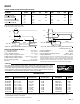
CONTROL LOGIC
The AD1674 may be operated in one of two modes, the full-
control mode and the stand-alone mode. The full-control mode
utilizes all the AD1674 control signals and is useful in systems
that address decode multiple devices on a single data bus. The
stand-alone mode is useful in systems with dedicated input ports
available and thus not requiring full bus interface capability.
Table I is a truth table for the AD1674, and Figure 10 illus-
trates the internal logic circuitry.
Table I. AD1674A Truth Table
CE CS R/C 12/8 A
0
Operation
0 X X X X None
X 1 X X X None
1 0 0 X 0 Initiate 12-Bit Conversion
1 0 0 X 1 Initiate 8-Bit Conversion
1 0 1 1 X Enable 12-Bit Parallel Output
1 0 1 0 0 Enable 8 Most Significant Bits
1 0 1 0 1 Enable 4 LSBs +4 Trailing Zeroes
REV. C
–9–
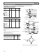
Figure 7. S/(N+D) vs. Input Amplitude
0
–130
50
–100
–120
5
–110
0
–70
–90
–80
–60
–40
–30
–10
–20
–50
4535301510
FREQUENCY – kHz
AMPLITUDE – dB
20 25 40
Figure 9. IMD Plot for f
IN
= 9.08 kHz (fa), 9.58 kHz (fb)
0
–140
50
–80
–120
5
–100
0
–20
–60
–40
4540353025201510
FREQUENCY – kHz
AMPLITUDE – dB
Figure 8. Nonaveraged 2048 Point FFT
at 100 kSPS, f
IN
= 25.049 kHz
INPUT FREQUENCY – kHz
S/(N+D) – dB
80
0
10000
20
10
101
40
30
50
60
70
1000
0dB INPUT
–20dB INPUT
–60dB INPUT
100
Figure 6. S/(N+D) vs. Input Frequency
and Amplitude