
Datasheet


AD1674
REV. C
–5–
(for all grades T
MIN
to T
MAX
with V
CC
= +15 V 6 10% or +12 V 6 5%,
V
LOGIC
= +5 V 610%, V
EE
= –15 V 6 10% or –12 V 6 5%; V
IL
= 0.4 V,
V
IH
= 2.4 V unless otherwise noted)
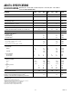
SWITCHING SPECIFICATIONS
CONVERTER START TIMING (Figure 1)
J, K, A, B, Grades T Grade
Parameter Symbol Min Typ Max Min Typ Max Units
Conversion Time
8-Bit Cycle t
C
78 78µs
12-Bit Cycle t
C
910 910µs
STS Delay from CE t
DSC
200 225 ns
CE Pulse Width t
HEC
50 50 ns
CS to CE Setup t
SSC
50 50 ns
CS Low During CE High t
HSC
50 50 ns
R/C to CE Setup t
SRC
50 50 ns
R/C Low During CE High t
HRC
50 50 ns
A
0
to CE Setup t
SAC
00ns
A
0
Valid During CE High t
HAC
50 50 ns
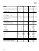
READ TIMING—FULL CONTROL MODE (Figure 2)
J, K, A, B, Grades T Grade
Parameter Symbol Min Typ Max Min Typ Max Units
Access Time t
DD
1
75 150 75 150 ns
Data Valid After CE Low t
HD
25
2
25
2
ns
20
3
15
4
ns
Output Float Delay t
HL
5
150 150 ns
CS to CE Setup t
SSR
50 50 ns
R/C to CE Setup t
SRR
00ns
A
0
to CE Setup t
SAR
50 50 ns
CS Valid After CE Low t
HSR
00ns
R/C High After CE Low t
HRR
00ns
A
0
Valid After CE Low t
HAR
50 50 ns
NOTES
1
t
DD
is measured with the load circuit of Figure 3 and is defined as the time
required for an output to cross 0.4 V or 2.4 V.
2
0°C to T
MAX
.
3
At –40°C.
4
At –55°C.
5
t
HL
is defined as the time required for the data lines to change 0.5 V when
loaded with the circuit of Figure 3.
All min and max specifications are guaranteed.
Specifications subject to change without notice.
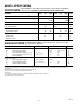
Test V
CP
C
OUT
Access Time High Z to Logic Low 5 V 100 pF
Float Time Logic High to High Z 0 V 10 pF
Access Time High Z to Logic High 0 V 100 pF
Float Time Logic Low to High Z 5 V 10 pF
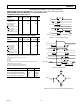
t
HEC
CE
STS
DB11 – DB0
A
0
CS
__
R/C
_
t
SSC
t
HSC
t
SRC
t
HRC
t
SAC
t
HAC
t
C
t
DSC
HIGH IMPEDANCE
Figure 1. Converter Start Timing
HIGH
IMPEDANCE
CE
STS
DB11 – DB0
A
0
CS
__
R/C
_
t
HSR
t
SSR
t
HRR
t
SAR
t
HAR
t
DD
t
HL
HIGH
IMP.
DATA
VALID
t
HD
t
HS
t
SSR
Figure 2. Read Timing
V
CP
D
OUT
C
OUT
I
OH
I
OL
Figure 3. Load Circuit for Bus Timing Specifications