
Datasheet


AD1851/AD1861
REV. A
–4–
ABSOLUTE MAXIMUM RATINGS*
V
L
to DGND . . . . . . . . . . . . . . . . . . . . . . . . . . . 0 V to 6.50 V
V
S
to AGND . . . . . . . . . . . . . . . . . . . . . . . . . . . 0 V to 6.50 V
–V
S
to AGND . . . . . . . . . . . . . . . . . . . . . . . . . –6.50 V to 0 V
Digital Inputs to DGND . . . . . . . . . . . . . . . . . . . –0.3 V to V
L
AGND to DGND . . . . . . . . . . . . . . . . . . . . . . . . . . . . ±0.3 V
Short Circuit . . . . . . . . . . . . . . . . .Indefinite Short to Ground
Soldering . . . . . . . . . . . . . . . . . . . . . . . . . . . . .+300°C, 10 sec
Storage Temperature . . . . . . . . . . . . . . . . . . –60°C to +100°C
*Stresses greater than those listed under “Absolute Maximum Ratings” may cause
permanent damage to the device. This is a stress rating only and functional
operation of the device at these or any other conditions above those indicated in the
operational section of this specification is not implied. Exposure to absolute
maximum rating conditions for extended periods may affect device reliability.
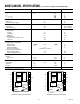
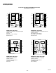
PIN DESCRIPTIONS
1–V
S
Analog Negative Power Supply
2 DGND Logic Ground
3V
L
Logic Positive Power Supply
4 NC No Connection
5 CLK Clock Input
6 LE Latch Enable Input
7 DATA Serial Data Input
8 NC No Internal Connection*
9V
OUT
Voltage Output
10 R
F
Feedback Resistor
11 SJ Summing Junction
12 AGND Analog Ground
13 I
OUT
Current Output
14 MSB ADJ MSB Adjustment Terminal
15 TRIM MSB Trimming Potentiometer Terminal
16 V
S
Analog Positive Power Supply
*Pin 8 has no internal connection; -V
L
from AD1856 or AD1860 socket can be
safely applied.
ORDERING GUIDE
Package
Model Resolution THD + N Option*
AD1851N 16 Bits 0.008% N-16
AD1851N-J 16 Bits 0.004% N-16
AD1851R 16 Bits 0.008% R-16
AD1851R-J 16 Bits 0.004% R-16
AD1861N 18 Bits 0.008% N-16
AD1861N-J 18 Bits 0.004% N-16
AD1861R 18 Bits 0.008% R-16
AD1861R-J 18 Bits 0.004% R-16
*N = Plastic DIP Package; R = Small Outline (SOIC) Package.
CAUTION
ESD (electrostatic discharge) sensitive device. The digital control inputs are diode protected;
however, permanent damage may occur on unconnected devices subject to high energy electro-
static fields. Unused devices must be stored in conductive foam or shunts. The protective foam
should be discharged to the destination socket before devices are inserted.
WARNING!
ESD SENSITIVE DEVICE
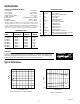
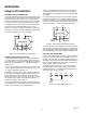
Typical Performance
175
150
125
100
75
50
25
2 4 6 8 10 12 14
CLOCK FREQUENCY – MHz
PD – mW
Power Dissipation vs. Clock Frequency
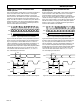
THD+N – %
10
1
0.1
0.01
0.001
–30 –20 –10 0 10 20 30 40 50 60 70 80 90
TEMPERATURE –
°
C
–60dB
–20dB
0dB
THD vs. Temperature