
Datasheet

AD1939 Data Sheet
Rev. E | Page 14 of 32
master clock. In addition, it is especially important that the
clock signal not pass through an FPGA, CPLD, or other large
digital chip (such as a DSP) before being applied to the
AD1939. In most cases, this induces clock jitter due to the
sharing of common power and ground connections with other
unrelated digital output signals. When the PLL is used, jitter in
the reference clock is attenuated above a certain frequency
depending on the loop filter.
RESET AND POWER-DOWN
The function of the
RST
pin sets all the control registers to their
default settings. To avoid pops, reset does not power down the
analog outputs. After
RST
is deasserted and the PLL acquires
lock condition, an initialization routine runs inside the
AD1939. This initialization lasts for approximately 256 master
clock cycles.
The power-down bits in the PLL and Clock Control 0, DAC
Control 1, and ADC Control 1 registers power down the
respective sections. All other register settings are retained. To
guarantee proper startup, the
RST
pin should be pulled low by
an external resistor.
SERIAL CONTROL PORT
The AD1939 has an SPI control port that permits programming
and reading back of the internal control registers for the ADCs,
DACs, and clock system. A standalone mode is also available
for operation without serial control; standalone is configured at
reset by connecting CIN, CCLK, and
CLATCH
to ground. In
standalone mode, all registers are set to default, except the
internal MCLK enable, which is set to 1. The ADC, ABCLK, and
ALRCLK clock ports are set to master/slave by the connecting
the COUT pin to either DVDD or ground. Standalone mode
only supports stereo mode with an I2S data format and 256 f
S
MCLK rate. Refer to Table 11 for details. If CIN, CCLK, and
CLATCH
are not grounded, the AD1939 SPI port is active. It is
recommended to use a weak pull-up resistor on
CLATCH
in
applications that have a microcontroller. This pull-up resistor
ensures that the AD1939 recognizes the presence of a
microcontroller.
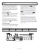
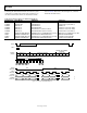
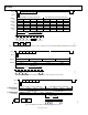
The SPI control port of the AD1939 is a 4-wire serial control
port. The format is similar to the Motorola SPI format except
the input data-word is 24 bits wide. The serial bit clock and
latch can be completely asynchronous to the sample rate of the
ADCs and DACs. Figure 11 shows the format of the SPI signal.
The first byte is a global address with a read/write bit. For the
AD1939, the address is 0x04, shifted left one bit due to the R/
W
bit. The second byte is the AD1939 register address and the
third byte is the data.
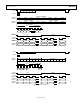
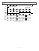
Table 11. Standalone Mode Selection
ADC Clocks CIN COUT CCLK
CLATCH
Slave 0 0 0 0
Master 0 1 0 0
D0
D0
D8
D8
D22D23 D9
D9
C
LATCH
CCLK
CIN
COUT
t
CCH
t
CCL
t
CDS
t
CDH
t
CLS
t
CCP
t
CLH
t
COTS
t
COD
t
COE
06071-010
Figure 11. Format of the SPI Signal