
Datasheet


AD22057
–8–
REV. A
PRINTED IN U.S.A.
AD22057
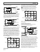
A1
A2
+V
S
R12
100kV
A2
C1
5pF
R1
200kV
R18
1kV
A1
R19 1kV
C2
5pF
R4
41kV
R9
10kV
R7
250V
R17
95kV
R15
10kV
OUT
R16
10kV
R14
20kV
R13
20kV
R5
2.6kV
R3
41kV
GND
OFS
R6
250kV
R8
9kV
R2
200kV
R11
2kV
R10
2kV
IN+
IN–
Figure 16. Simplified Schematic of AD22057, Including Component Values
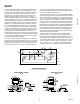
OUTLINE DIMENSIONS
Dimensions shown in inches and (mm).
Plastic SOIC Package
(SO-8)
0.1968 (5.00)
0.1890 (4.80)
8
5
41
0.2440 (6.20)
0.2284 (5.80)
PIN 1
0.1574 (4.00)
0.1497 (3.80)
0.0688 (1.75)
0.0532 (1.35)
SEATING
PLANE
0.0098 (0.25)
0.0040 (0.10)
0.0192 (0.49)
0.0138 (0.35)
0.0500
(1.27)
BSC
0.0098 (0.25)
0.0075 (0.19)
0.0500 (1.27)
0.0160 (0.41)
88
08
0.0196 (0.50)
0.0099 (0.25)
3 458
Plastic Mini-DIP Package
(N-8)
8
14
5
0.430 (10.92)
0.348 (8.84)
0.280 (7.11)
0.240 (6.10)
PIN 1
SEATING
PLANE
0.022 (0.558)
0.014 (0.356)
0.060 (1.52)
0.015 (0.38)
0.210 (5.33)
MAX
0.130
(3.30)
MIN
0.070 (1.77)
0.045 (1.15)
0.100
(2.54)
BSC
0.160 (4.06)
0.115 (2.93)
0.325 (8.25)
0.300 (7.62)
0.015 (0.381)
0.008 (0.204)
0.195 (4.95)
0.115 (2.93)
C2181a–2–4/99
A unique method of feedback around A1, provided by R9 and
R7, sets the closed-loop gain of the preamplifier to ×10 (from
the input pins). The feedback network is balanced by the inclu-
sion of R6 and R8. The small value of R7 results in a more
practical value for R9 (which would have to be 2 MΩ if the
feedback were taken directly to the inputs of A1). R8 is not
directly connected to ground, but to an optional voltage of one
half that is applied to Pin 7 (OFS). It is trimmed to within close
tolerances through R10 and R11. This allows the output of A1
to be offset to midscale, typically +V
S
/2, by tying Pins 6 and 7
together. (For an example of the use of this feature, see Figure
12.) The gain is adjusted by the single resistor R5, which acts
only on the differential signal. More importantly, it also results
in much less feed forward of the common-mode signal to the
output of A1, which, being a single-supply circuit, has no means
of pulling this output down toward ground in those circum-
stances where the common-mode input is very positive while the
net differential signal is small. (The output of A1 is the collector
of a PNP transistor whose emitter is tied to +V
S
.) R16 is specifi-
cally included to alleviate this problem.
The output of the preamplifier is connected to Pin 3 via R12, a
100 kΩ resistor that is trimmed to within ±3%. The inclusion of
R12 allows a low-pass filter to be formed, with an accurate time
constant, by placing a capacitor from Pin 3 to ground. By sepa-
rating the connections at Pins 3 and 4, a two-pole Sallen and
Key filter can be formed (see Low-Pass Filtering section) and
also provides a means for setting the overall gain to values other
than ×20 (see Altering the Gain section).
The output buffer has a gain of ×2, set by the feedback network
around op amp A2, formed by R15 and R13储R14. Note that this
gain is not trimmed to a precise value, but may have a tolerance
of ±3% (max). Only the overall gain of A1 and A2 is trimmed to
within ±0.5% by R5. As a consequence, the gain of A1 may be
in error by ±3% (max) as the trim to R5 absorbs the initial error
in the gain of A2. In most applications Pins 3 and 4 are simply
tied together, but the output buffer can be used independently if
desired. The offset voltage of A2 is nulled during manufacture.
R17 is included to minimize the offset due to bias currents. It is
recommended, in applications where A2 is used independently
and the source resistance is less than 100 kΩ, that the necessary
extra resistance should be included.
The output of A2 is the collector of a PNP transistor whose
emitter is tied to +V
S
. The bias current out of the inverting
input of this amplifier generates an offset voltage of about +1 mV
in R13储R14, which is passed directly to the output via R15. This
sets the lowest output that can be reached when there is no load
resistor. However, the output can drive a 1 kΩ load to at least
+4.5 V when +V
S
= +5 V. If operation to much lower minimum
voltages is essential, a load resistor can be added externally.