
Datasheet


AD2S1205
Rev. A | Page 2 of 20
TABLE OF CONTENTS
Features .............................................................................................. 1
Applications ....................................................................................... 1
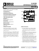
Functional Block Diagram .............................................................. 1
General Description ......................................................................... 1
Product Highlights ........................................................................... 1
Revision History ............................................................................... 2
Specifications ..................................................................................... 3
Absolute Maximum Ratings ............................................................ 5
ESD Caution .................................................................................. 5
Pin Configuration and Function Descriptions ............................. 6
Resolver Format Signals ................................................................... 8
Theory of Operation ........................................................................ 9
Fault Detection Circuit ................................................................ 9
Monitor Signal .............................................................................. 9
Loss of Signal Detection .............................................................. 9
Signal Degradation Detection .................................................. 10
Loss of Position Tracking Detection ........................................ 10
Responding to a Fault Condition ............................................. 10
False Null Condition .................................................................. 10
On-Board Programmable Sinusoidal Oscillator .................... 11
Synthetic Reference Generation ............................................... 11
Charge-Pump Output ................................................................ 11
Connecting the Converter ........................................................ 11
Clock Requirements ................................................................... 12
Absolute Position and Velocity Output ................................... 12
Parallel Interface ......................................................................... 12
Serial Interface ............................................................................ 14
Incremental Encoder Outputs .................................................. 16
Supply Sequencing and Reset ................................................... 16
Circuit Dynamics ........................................................................... 17
Loop Response Model ............................................................... 17
Sources of Error .......................................................................... 18
Connecting to the DSP .............................................................. 19
Outline Dimensions ....................................................................... 20
Ordering Guide .......................................................................... 20
Automotive Products ................................................................. 20
REVISION HISTORY
5/10—Rev. 0 to Rev. A
Changes to Features Section............................................................ 1
Changes to Input Bias Current Parameter and Input
Impedance Parameter ...................................................................... 3
Changes to Table 2 ............................................................................ 5
Changes to Loss of Signal Detection Section ................................ 9
Changes to Connecting the Converter Section and Figure 5 ... 11
Change to t
6
Max Value in Table 6 ............................................... 13
Changes to t
9
and t
10
Max Values Table 7 .................................... 15
Changes to Ordering Guide .......................................................... 20
Added Automotive Products Section .......................................... 20
1/07—Revision 0: Initial Version