
Datasheet


AD2S1205
Rev. A | Page 7 of 20
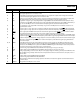
Pin No. Mnemonic Description
26 B
Incremental Encoder Emulation Output B. Logic output. This output is free running and is valid if the resolver format
input signals applied to the converter are valid.
27 NM
North Marker Incremental Encoder Emulation Output. Logic output. This output is free running and is valid if the
resolver format input signals applied to the converter are valid.
28 DIR
Direction. Logic output. This output is used in conjunction with the incremental encoder emulation outputs. The
DIR output indicates the direction of the input rotation and is high for increasing angular rotation.
29 DOS
Degradation of Signal. Logic output. Degradation of signal (DOS) is detected when either resolver input (Sin or Cos)
exceeds the specified DOS Sin/Cos threshold. See the Signal Degradation Detection section. DOS is indicated by a
logic low on the DOS pin and is not latched when the input signals exceed the maximum input level.
30 LOT
Loss of Tracking. Logic output. LOT is indicated by a logic low on the LOT pin and is not latched. See the Loss of
Signal Detection section.
31 FS1
Frequency Select 1. Logic input. FSI in conjunction with FS2 allows the frequency of EXC/EXC
to be programmed.
32 FS2
Frequency Select 2. Logic input. FS2 in conjunction with FS1 allows the frequency of EXC/EXC
to be programmed.
33
RESET
Reset. Logic input. The AD2S1205 requires an external reset signal to hold the RESET input low until V
DD
is within
the specified operating range of 4.5 V to 5.5 V. See the section. Supply Sequencing and Reset
34 EXC
Excitiation Frequency. Analog output. An on-board oscillator provides the sinusoidal excitation signal (EXC) and its
complement signal (EXC
) to the resolver. The frequency of this reference signal is programmable via the FS1 and FS2 pins.
35
EXC
Excitation Frequency Complement. Analog output. An on-board oscillator provides the sinusoidal excitation signal
(EXC) and its complement signal (EXC
) to the resolver. The frequency of this reference signal is programmable via
the FS1 and FS2 pins.
36, 42 AGND
Analog Ground. These pins are ground reference points for analog circuitry on the AD2S1205. All analog input
signals and any external reference signal should be referred to this AGND voltage. Both of these pins should be
connected to the AGND plane of a system. The AGND and DGND voltages should ideally be at the same potential
and must not be more than 0.3 V apart, even on a transient basis.
37 Sin Positive Analog Input of Differential Sin/SinLO Pair. The input range is 2.3 V p-p to 4.0 V p-p.
38 SinLO Negative Analog Input of Differential Sin/SinLO Pair. The input range is 2.3 V p-p to 4.0 V p-p.
39 AV
DD
Analog Supply Voltage, 4.75 V to 5.25 V. This pin is the supply voltage for all analog circuitry on the AD2S1205. The
AV
DD
and DV
DD
voltages ideally should be at the same potential and must not be more than 0.3 V apart, even on a
transient basis.
40 CosLO Negative Analog Input of Differential Cos/CosLO Pair.
41 Cos Positive Analog Input of Differential Cos/CosLO Pair.
43 REFBYP
Reference Bypass. Reference decoupling capacitors should be connected here. Typical recommended values are
10 μF and 0.01 μF.
44 REFOUT Voltage Reference Output, 2.39 V to 2.52 V.