
Datasheet

AD2S1205
Rev. A | Page 12 of 20
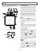
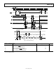
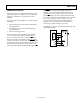
A separate screened twisted pair cable is recommended for
analog inputs Sin/SinLO and Cos/CosLO. The screens should
terminate to either REFOUT or AGND.
06339-005
DV
DD
5V
1
2
3
4
5
6
7
8
9
10
11
RESET
33
32
31
30
29
28
27
26
25
24
DGND
8.192
MHz
20pF20pF
4.7μF 10nF
23
12 13 14 15
DGND
16
DV
DD
17 18 19 20 21 22
44
REFBYP
43
AGND
42
Cos
41
CosLO
40
AV
DD
39
SinLO
38
Sin
37
AGND
36 35
EXC
34
AD2S1205
EXC
10μF
10nF
5V
S2
S4
4.7μF
10nF
S3
S1
5V
BUFFER
CIRCUIT
BUFFER
CIRCUIT
R2
R1
68kΩ 68kΩ
Figure 5. Connecting the AD2S1205 to a Resolver
06339-017
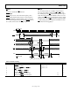
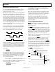
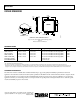
C1
R2
R1
12V
12V
5V
EXC/EXC
(V
IN
)
(V
REF
)
V
OUT
AD8662
Figure 6. Buffer Circuit
CLOCK REQUIREMENTS
To achieve the specified dynamic performance, an external crystal
is recommended at the CLKIN and XTALOUT pins. The position
and velocity accuracy are guaranteed for a frequency range of
8.192 MHz ± 25%. However, the velocity outputs are scaled in
proportion to the clock frequency so that if the clock is 25%
greater than the nominal, the full-scale velocity is 25% greater than
nominal. The maximum tracking rate, tracking loop bandwidth,
and excitation frequency also vary with the clock frequency.
ABSOLUTE POSITION AND VELOCITY OUTPUT
The angular position and velocity are represented by binary data
and can be extracted via either a 12-bit parallel interface or a
3-wire serial interface that operates at clock rates of up to 25 MHz.
SOE
Input
The serial output enable pin (
SOE
) is held high to enable the
parallel interface and low to enable the serial interface. In the
latter case, Pin DB0 to Pin DB9 are placed into a high impedance
state while DB11 is the serial output (SO) and DB10 is the serial
clock input (SCLK).
Data Format
The angular position data represents the absolute position of
the resolver shaft as a 12-bit unsigned binary word. The angular
velocity data is a 12-bit twos complement word, representing
the velocity of the resolver shaft rotating in either a clockwise
or counterclockwise direction.
PARALLEL INTERFACE
The angular position and velocity are available on the AD2S1205
in two 12-bit registers, accessed via the 12-bit parallel port. The
parallel interface is selected by holding the
SOE
pin high. Data
is transferred from the velocity and position integrators to the
position and velocity registers, respectively, after a high-to-low
transition on the
SAMPLE
pin. The
RDVEL
pin selects whether
data from the position or velocity register is transferred to the
output register. The
CS
pin must be held low to transfer data
from the selected register to the output register. Finally, the
RD
input is used to read the data from the output register and to
enable the output buffer. The timing requirements for the read
cycle are shown in . Figure 7
SAMPLE
Input
Data is transferred from the position and velocity integrators to
the position and velocity registers, respectively, after a high-to-
low transition on the
SAMPLE
signal. This pin must be held
low for at least t
1
to guarantee correct latching of the data.
RD
should not be pulled low before this time because data will not
be ready. The converter continues to operate during the read
process. A rising edge of
SAMPLE
resets the internal registers
that contain the minimum and maximum magnitude of the
monitor signal.