
Datasheet

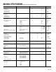


AD2S80A–SPECIFICATIONS
Parameter Conditions Min Typ Max Unit
RATIO MULTIPLIER
AC Error Output Scaling 10 Bit 177.6 mV/Bit
12 Bit 44.4 mV/Bit
14 Bit 11.1 mV/Bit
16 Bit 2.775 mV/Bit
PHASE SENSITIVE DETECTOR
Output Offset Voltage 12 mV
Gain
In Phase w.r.t. REF –0.882 –0.9 –0.918 V rms/V dc
In Quadrature w.r.t. REF ±0.02 V rms/V dc
Input Bias Current 60 150 nA
Input Impedance 1 MΩ
Input Voltage ±8V
INTEGRATOR
Open-Loop Gain At 10 kHz 57 63 dB
Dead Zone Current (Hysteresis) 100 nA/LSB
Input Offset Voltage 15 mV
Input Bias Current 60 150 nA
Output Voltage Range ±V
S
= ±10.8 V dc ±7V
VCO
Maximum Rate ±V
S
= ±12 V dc 1.1 MHz
VCO Rate Positive Direction 7.1 7.9 8.7 kHz/µA
Negative Direction 7.1 7.9 8.7 kHz/µA
VCO Power Supply Sensitivity
Increase +V
S
+0.5 %/V
–V
S
–8.0 %/V
Decrease +V
S
–8.0 %/V
–V
S
+2.0 %/V
Input Offset Voltage 15 mV
Input Bias Current 70 380 nA
Input Bias Current Tempco –1.22 nA/°C
Input Voltage Range ±8V
Linearity of Absolute Rate
Full Range <2 % FSD
Over 0% to 50% of Full Range <1 % FSD
Reversion Error 1.5 % FSD
Sensitivity of Reversion Error ±8 %/V of
to Symmetry of Power Supplies Asymmetry
POWER SUPPLIES
Voltage Levels
+V
S
+10.8 +13.2 V
–V
S
–10.8 –13.2 V
+V
L
+5 +13.2 V
Current
±I
S
±V
S
@ ±12 V ⴞ12 ⴞ23 mA
±I
S
±V
S
@ 13.2 V ⴞ19 ⴞ30 mA
±I
L
+V
L
@ ±5.0 V ⴞ0.5 ⴞ1.5 mA
Specification subject to change without notice.
All min and max specifications are guaranteed. Specifications in boldface are tested on all production units at final electrical test.
(typical at 25
ⴗ
C unless otherwise noted)
–4–
REV. B
CAUTION
ESD (electrostatic discharge) sensitive device. Electrostatic charges as high as 4000 V readily
accumulate on the human body and test equipment and can discharge without detection. Although
the AD2S80A features proprietary ESD protection circuitry, permanent damage may occur on
devices subjected to high-energy electrostatic discharges. Therefore, proper ESD precautions are
recommended to avoid performance degradation or loss of functionality.
WARNING!
ESD SENSITIVE DEVICE