
Datasheet


AD5063
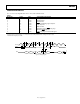
Rev. C | Page 4 of 20
B Version
1
Parameter Min Typ Max Unit Test Conditions/Comments
POWER REQUIREMENTS
V
DD
2.7 5.5 V All digital inputs at 0 V or V
DD
I
DD
(Normal Mode) DAC active and excluding load current
V
DD
= 4.5 V to 5.5 V 0.65 0.7 mA
V
IN
= V
DD
and V
IL
= GND, V
DD
= 5 V,
V
REF
= 4.096 V, code = midscale
V
DD
= 2.7 V to 3.6 V 0.5 mA V
IH
= V
DD
and V
IL
= GND, V
DD
= 3 V
I
DD
(All Power-Down Modes)
V
DD
= 4.5 V to 5.5 V 1 μA V
IH
= V
DD
and V
IL
= GND
V
DD
= 2.7 V to 3.6 V 1 μA V
IH
= V
DD
and V
IL
= GND
Power Supply Rejection Ratio (PSRR) 0.5 LSB ∆V
DD
± 10%, V
DD
= 5 V, unloaded
1
Temperature ranges for the B version: −40°C to +85°C, typical at +25°C, functional to +125°C.
2
Guaranteed by design and characterization, not production tested.
3
See the Ordering Guide.
4
Total current flowing into all pins.