
Datasheet


AD5063
Rev. C | Page 6 of 20
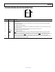
ABSOLUTE MAXIMUM RATINGS
Table 4.
Parameter Rating
V
DD
to GND −0.3 V to +7.0 V
Digital Input Voltage to GND −0.3 V to V
DD
+ 0.3 V
V
OUT
to GND −0.3 V to V
DD
+ 0.3 V
V
REF
to GND −0.3 V to V
DD
+ 0.3 V
INV to GND −0.3 V to V
DD
+ 0.3 V
R
FB
to GND +7 V to −7 V
Operating Temperature Range
Industrial (B Version) −40°C to + 85°C
1
Storage Temperature Range −65°C to +150°C
Maximum Junction Temperature 150°C
MSOP Package
Power Dissipation (T
J
max − T
A
)/θ
JA
θ
JA
Thermal Impedance 206°C/W
θ
Jc
Thermal Impedance 44°C/W
Reflow Soldering (Pb-Free)
Peak Temperature 260(0/−5)°C
Time at Peak Temperature 10 sec to 40 sec
ESD 1.5 kV
1
Temperature range for this device is −40°C to +85°C; however, the device is
still operational at 125°C.
Stresses above those listed under Absolute Maximum Ratings
may cause permanent damage to the device. This is a stress
rating only; functional operation of the device at these or any
other conditions above those indicated in the operational
section of this specification is not implied. Exposure to absolute
maximum rating conditions for extended periods may affect
device reliability.
This device is a high performance integrated circuit with an
ESD rating of <2 kV, and it is ESD sensitive. Proper precautions
should be taken for handling and assembly.
ESD CAUTION
ESD (electrostatic discharge) sensitive device. Electrostatic charges as high as 4000 V readily accumulate on
the human body and test equipment and can discharge without detection. Although this product features
proprietary ESD protection circuitry, permanent damage may occur on devices subjected to high energy
electrostatic discharges. Therefore, proper ESD precautions are recommended to avoid performance
degradation or loss of functionality.