
Datasheet


AD5063
Rev. C | Page 7 of 20
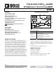
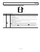
PIN CONFIGURATION AND FUNCTION DESCRIPTIONS
AD5063
TOP VIEW
(Not to Scale)
V
OUT
SYNC
110
AGND
SCLK
29
DIN
DACGND
38
04766-003
V
REF
47
V
DD
INV
R
FB
56
Figure 3. Pin Configuration
Table 5. Pin Function Descriptions
Pin No. Mnemonic Description
1 DIN
Serial Data Input. This device has a 24-bit shift register. Data is clocked into the register on the falling edge of the
serial clock input.
2 V
DD
Power Supply Input. These parts can be operated from 2.7 V to 5.5 V, and V
DD
should be decoupled to GND.
3 V
REF
Reference Voltage Input.
4 V
OUT
Analog Output Voltage from DAC.
5 INV
Connected to the Internal Scaling Resistors of the DAC. Connect the INV pin to the external op amp’s inverting
input in bipolar mode.
6 R
FB
Feedback Resistor. In bipolar mode, connect this pin to the external op amp circuit.
7 AGND Ground Reference Point for Analog Circuitry.
8 DACGND Ground Input to the DAC.
9
SYNC
Level-Triggered Control Input (Active Low). This is the frame synchronization signal for the input data. When
SYNC
goes low, it enables the input shift register, and data is then transferred in on the falling edges of the
following clocks. The DAC is updated following the 24
th
clock cycle unless SYNC is taken high before this edge, in
which case the rising edge of SYNC
acts as an interrupt, and the write sequence is ignored by the DAC.
10 SCLK
Serial Clock Input. Data is clocked into the input shift register on the falling edge of the serial clock input. Data
can be transferred at rates of up to 30 MHz.