
Datasheet


AD5123/AD5143 Data Sheet
Rev. A | Page 2 of 28
TABLE OF CONTENTS
Features .............................................................................................. 1
Applications ....................................................................................... 1
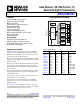
Functional Block Diagram .............................................................. 1
General Description ......................................................................... 1
Revision History ............................................................................... 2
Specifications ..................................................................................... 3
Electrical Characteristics—AD5123 .......................................... 3
Electrical Characteristics—AD5143 .......................................... 6
Interface Timing Specifications .................................................. 9
Shift Register and Timing Diagrams ....................................... 10
Absolute Maximum Ratings .......................................................... 11
Thermal Resistance .................................................................... 11
ESD Caution ................................................................................ 11
Pin Configuration and Function Descriptions ........................... 12
Typical Performance Characteristics ........................................... 13
Test Circuits ..................................................................................... 18
Theory of Operation ...................................................................... 19
RDAC Register and EEPROM .................................................. 19
Input Shift Register .................................................................... 19
I
2
C Serial Data Interface ............................................................ 19
I
2
C Address .................................................................................. 19
Advanced Control Modes ......................................................... 21
EEPROM or RDAC Register Protection ................................. 22
RDAC Architecture .................................................................... 25
Programming the Variable Resistor ......................................... 25
Programming the Potentiometer Divider ............................... 26
Terminal Voltage Operating Range ......................................... 26
Power-Up Sequence ................................................................... 26
Layout and Power Supply Biasing ............................................ 26
Outline Dimensions ....................................................................... 27
Ordering Guide .......................................................................... 27
REVISION HISTORY
3/13—Rev. 0 to Rev. A
Changes to Features Section............................................................ 1
10/12—Revision 0: Initial Version