
Datasheet


Data Sheet AD5123/AD5143
Rev. A | Page 9 of 28
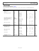
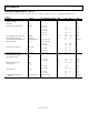
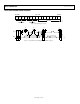
INTERFACE TIMING SPECIFICATIONS
V
DD
= 2.3 V to 5.5 V; all specifications T
MIN
to T
MAX
, unless otherwise noted.
Table 4. I
2
C Interface
Parameter
1
Test Conditions/Comments Min Typ Max Unit Description
f
SCL
2
Standard mode 100 kHz Serial clock frequency
Fast mode 400 kHz
t
1
Standard mode 4.0 µs SCL high time, t
HIGH
Fast mode 0.6 µs
t
2
Standard mode 4.7 µs SCL low time, t
LOW
Fast mode 1.3 µs
t
3
Standard mode 250 ns Data setup time, t
SU; DAT
Fast mode 100 ns
t
4
Standard mode 0 3.45 µs Data hold time, t
HD; DAT
Fast mode 0 0.9 µs
t
5
Standard mode 4.7 µs Setup time for a repeated start condition, t
SU; STA
Fast mode 0.6 µs
t
6
Standard mode 4 µs Hold time (repeated) for a start condition, t
HD; STA
Fast mode 0.6 µs
t
7
Standard mode 4.7 µs Bus free time between a stop and a start condition, t
BUF
Fast mode
1.3
µs
t
8
Standard mode 4 µs Setup time for a stop condition, t
SU; STO
Fast mode 0.6 µs
t
9
Standard mode 1000 ns Rise time of SDA signal, t
RDA
Fast mode 20 + 0.1 C
L
300 ns
t
10
Standard mode 300 ns Fall time of SDA signal, t
FDA
Fast mode 20 + 0.1 C
L
300 ns
t
11
Standard mode 1000 ns Rise time of SCL signal, t
RCL
Fast mode 20 + 0.1 C
L
300 ns
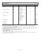
t
11A
Standard mode 1000 ns Rise time of SCL signal after a repeated start condition
and after an acknowledge bit, t
RCL1
(not shown in Figure 3)
Fast mode 20 + 0.1 C
L
300 ns
t
12
Standard mode
300
ns
Fall time of SCL signal, t
FCL
Fast mode 20 + 0.1 C
L
300 ns
t
SP
3
Fast mode 0 50 ns Pulse width of suppressed spike (not shown in Figure 3)
t
EEPROM_PROGRAM
4
15 50 ms Memory program time (not shown in Figure 3)
t
EEPROM_READBACK
7 30 µs Memory readback time (not shown in Figure 3)
t
POWER_UP
5
75 µs Power-on EEPROM restore time (not shown in Figure 3)
t
RESET
30 µs Reset EEPROM restore time (not shown in Figure 3)
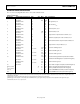
1
Maximum bus capacitance is limited to 400 pF.
2
The SDA and SCL timing is measured with the input filters enabled. Switching off the input filters improves the transfer rate; however, it has a negative effect on the
EMC behavior of the part.
3
Input filtering on the SCL and SDA inputs suppresses noise spikes that are less than 50 ns for fast mode.
4
EEPROM program time depends on the temperature and EEPROM write cycles. Higher timing is expected at lower temperatures and higher write cycles.
5
Maximum time after V
DD
− V
SS
is equal to 2.3 V.