
Datasheet


AD5124/AD5144/AD5144A Data Sheet
Rev. A | Page 10 of 36
INTERFACE TIMING SPECIFICATIONS
V
LOGIC
= 1.8 V to 5.5 V; all specifications T
MIN
to T
MAX
, unless otherwise noted.
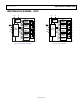
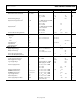
Table 4. SPI Interface
Parameter
1
Test Conditions/Comments Min Typ Max Unit Description
t
1
V
LOGIC
> 1.8 V 20 ns SCLK cycle time
V
LOGIC
= 1.8 V 30 ns
t
2
V
LOGIC
> 1.8 V 10 ns SCLK high time
V
LOGIC
= 1.8 V 15 ns
t
3
V
LOGIC
> 1.8 V 10 ns SCLK low time
V
LOGIC
= 1.8 V 15 ns
t
4
10 ns
SYNC
-to-SCLK falling edge setup time
t
5
5 ns Data setup time
t
6
5 ns Data hold time
t
7
10 ns
SYNC
rising edge to next SCLK fall ignored
t
8
2
20 ns Minimum
SYNC
high time
t
9
3
50 ns SCLK rising edge to SDO valid
t
10
500 ns
SYNC
rising edge to SDO pin disable
1
All input signals are specified with t
r
= t
f
= 1 ns/V (10% to 90% of V
DD
) and timed from a voltage level of (V
IL
+ V
IH
)/2.
2
Refer to t
EEPROM_PROGRAM
and
t
EEPROM_READBACK
for memory commands operations (see Table 6).
3
R
PULL_UP
= 2.2 kΩ to V
DD
with a capacitance load of 168 pF.
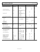
Table 5. I
2
C Interface
Parameter
1
Test Conditions/Comments Min Typ Max Unit Description
f
SCL
2
Standard mode
100
kHz
Serial clock frequency
Fast mode 400 kHz
t
1
Standard mode 4.0 µs SCL high time, t
HIGH
Fast mode 0.6 µs
t
2
Standard mode 4.7 µs SCL low time, t
LOW
Fast mode 1.3 µs
t
3
Standard mode 250 ns Data setup time, t
SU; DAT
Fast mode 100 ns
t
4
Standard mode 0 3.45 µs Data hold time, t
HD; DAT
Fast mode 0 0.9 µs
t
5
Standard mode 4.7 µs Setup time for a repeated start condition, t
SU; STA
Fast mode 0.6 µs
t
6
Standard mode 4 µs Hold time (repeated) for a start condition, t
HD; STA
Fast mode 0.6 µs
t
7
Standard mode 4.7 µs Bus free time between a stop and a start condition, t
BUF
Fast mode 1.3 µs
t
8
Standard mode 4 µs Setup time for a stop condition, t
SU; STO
Fast mode
0.6
µs
t
9
Standard mode 1000 ns Rise time of SDA signal, t
RDA
Fast mode 20 + 0.1 C
L
300 ns
t
10
Standard mode 300 ns Fall time of SDA signal, t
FDA
Fast mode 20 + 0.1 C
L
300 ns
t
11
Standard mode 1000 ns Rise time of SCL signal, t
RCL
Fast mode 20 + 0.1 C
L
300 ns
t
11A
Standard mode 1000 ns Rise time of SCL signal after a repeated start condition
and after an acknowledge bit, t
RCL1
(not shown in Figure 5)
Fast mode 20 + 0.1 C
L
300 ns