
Datasheet

REV. 0
AD5207
–10–
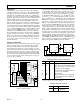
The data setup and data hold times in the specification table
determine the data valid time requirements. The last ten bits of
the data word entered into the serial register are held when CS
returns high and any extra bits are ignored. At the same time, when
CS goes high, it gates the address decoder enabling one of two
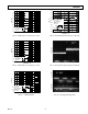
positive edge-triggered AD5207 RDAC latches; see Figure 5 detail.
SDI
CLK
CS
CK
RS
D
Q
SERIAL
REGISTER
SDO
SHDN
INTERNAL
RS
Figure 4. Detail SDO Output Schematic of the AD5207
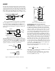
The target RDAC latch is loaded with the last eight bits of the
data word to complete one RDAC update. For AD5207, it
cannot update both channels simultaneously and therefore, two
separate 10-bit data words must be clocked in to change both
VR settings.
RDAC1
RDAC2
ADDR
DECODE
SERIAL
REGISTER
AD5207
SDI
CLK
CS
Figure 5. Equivalent Input Control Logic
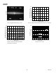
All digital inputs are protected with a series input resistor and
parallel Zener ESD structure shown in Figures 6 and 7. Applies
to digital input pins CS, SDI, SDO, SHDN, and CLK. Digital
input level for Logic 1 can be anywhere from 2.4 V to 5 V
regardless of whether it is in single or dual supplies.
340
V
SS
LOGIC
DIGITAL PIN
Figure 6. ESD Protection of Digital Pins
A,B,W
V
SS
Figure 7. ESD Protection of Resistor Terminals
D7
D6
D5
D4
D3
D2
D1
D0
RDAC
LATCH
AND
DECODER
R
S
R
S
R
S
R
S
SHDN
Ax
Wx
Bx
Figure 8. Equivalent RDAC Circuit
PROGRAMMING THE VARIABLE RESISTOR
Rheostat Operation
The nominal resistance of the RDAC between Terminals A and
B is available with values of 10 kΩ, 50 kΩ, and 100 kΩ. The last
few digits of the part number determine the nominal resistance
value, e.g., 10 kΩ = 10; 50 kΩ = 50; and 100 kΩ = 100. The
nominal resistance (R
AB
) of the VR has 256 contact points
accessed by the wiper terminal, plus the B Terminal contact.
The 8-bit data in the RDAC latch is decoded to select one of
the 256 possible settings. Assume a 10 kΩ part is used, the
wiper’s first connection starts at the B Terminal for data 00
H
.
Since there is a 45 Ω wiper contact resistance, such connection
yields a minimum of 45 Ω resistance between Terminals W and
B. The second connection is the first tap point corresponds to
84 Ω (R
WB
= R
AB
/256 + R
W
= 39 Ω + 45 Ω) for data 01
H
. The
third connection is the next tap point representing 123 Ω (39 ×
2 + 45) for data 02
H
and so on. Each LSB value increase moves
the wiper up the resistor ladder until the last tap point is reached at
10006 Ω (R
AB
– 1 LSB + R
W
). Figure 8 shows a simplified dia-
gram of the equivalent RDAC circuit.
The general equation determining the programmable output
resistance between W and B is:
RD
D
RR
WB AB W
()
=×+
256
(1)
where D is the data contained in the 8-bit RDAC latch, and R
AB
is the nominal end-to-end resistance.
For example, R
AB
=10 kΩ, A Terminal can be open-circuit or
tied to W. The following output resistance R
WB
will be set for
the following RDAC latch codes.