
Datasheet


REV. 0
AD5207
–11–
Table IV.
DR
WB
(DEC) () Output State
255 10006 Full-Scale (R
AB
– 1 LSB + R
W
)
128 5045 Midscale
1841 LSB
0 45 Zero-Scale (Wiper Contact Resistance)
Note that in the zero-scale condition a finite wiper resistance of
45 Ω is present. Care should be taken to limit the current flow
between W and B in this state to a maximum current of no more
than 5 mA. Otherwise, degradation or possibly destruction of
the internal switch contacts can occur.
Similar to the mechanical potentiometer, the resistance of the
RDAC between the wiper W and Terminal A also produces a
digitally controlled resistance R
WA
. When these terminals are used,
the B Terminal should be let open or tied to the wiper terminal.
Setting the resistance value for R
WA
starts at a maximum value
of resistance and decreases as the data loaded in the latch is
increased in value. The general equation for this operation is:
RD
D
RR
WA AB W
()
=×+
256
256
–
(2)
For example, when R
AB
= 10 kΩ, B terminal is either open or
tied to W, the following output resistance, R
WA
, will be set for
the following RDAC latch codes.
Table V.
DR
WA
(DEC) () Output State
255 84 Full-Scale (R
AB
/256 + R
W
)
128 5045 Midscale
1 10006 1 LSB
0 10045 Zero-Scale
The typical distribution of R
AB
from channel to channel matches
within ±1%. Device-to-device matching is process-lot depen-
dent and is possible to have ±30% variation. The change in R
AB
with temperature has a 500 ppm/°C temperature coefficient.
PROGRAMMING THE POTENTIOMETER DIVIDER
Voltage Output Operation
The digital potentiometer easily generates an output voltage
proportional to the input voltage. Let’s ignore the effect of
the wiper resistance for the moment. For example, when con-
necting A Terminal to 5 V and B Terminal to ground, it produces
a programmable output voltage at the wiper starting at zero
volts up to 1 LSB less than 5 V. Each LSB of voltage is equal
to the voltage applied across terminal AB divided by the 256
position of the potentiometer divider. Since AD5207 is capable
for dual supplies, the general equation defining the output volt-
age with respect to ground for any given input voltage applied to
terminals AB is:
VD
D
V
D
V
WA B
()
=+
−
256
256
256
(3)
Operation of the digital potentiometer in the divider mode
results in more accurate operation over temperature. Unlike the
rheostat mode, the output voltage is dependent on the ratio of
R
WA
and R
WB
and not the absolute values; therefore, the drift
reduces to 15 ppm/°C. There is no voltage polarity constraint
between Terminals A, B, and W as long as the terminal voltage
stays within V
SS
< V
TERM
< V
DD
.
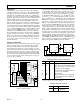
RDAC CIRCUIT SIMULATION MODEL
The internal parasitic capacitances and the external capacitive
loads dominate the ac characteristics of the RDACs. Config-
ured as a potentiometer divider the –3 dB bandwidth of the
AD5207BRU10 (10 kΩ resistor) measures 600 kHz at half
scale. TPC 16 provides the large signal BODE plot characteris-
tics of the three available resistor versions 10 kΩ and 50 kΩ.
The gain flatness versus frequency graph, TPC 16, predicts
filter applications performance. A parasitic simulation model has
been developed and is shown in Figure 9. Listing I provides a
macro model net list for the 10 kΩ RDAC:
C
W
70pF
C
B
C
A
B
A
RDAC
10k
W
C
B
= 45pFC
A
= 45pF
Figure 9. RDAC Circuit Simulation Model for RDAC = 10 k
Ω
Listing I. Macro Model Net List for RDAC
.PARAM D=255, RDAC=10E3
*
.SUBCKT DPOT (A,W)
*
CA A 0 45E-12
RAW A W {(1-D/256)*RDAC+50}
CW W 0 70E-12
RBW W B {D/256*RDAC+50}
CB B 0 45E-12
*
.ENDS DPOT