
Datasheet

REV. 0
–2–
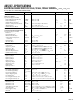
AD5207–SPECIFICATIONS
ELECTRICAL CHARACTERISTICS 10 k, 50 k, 100 k VERSION
(V
DD
= 5 V, V
SS
= 0, V
A
= 5 V,
V
B
= 0, –40C < T
A
< +125C unless otherwise noted.)
Parameter Symbol Conditions Min Typ
1
Max Unit
DC CHARACTERISTICS
RHEOSTAT MODE
Specifications Apply to All VRs
Resistor Differential Nonlinearity
2
R-DNL R
WB
, V
A
= NC –1 +1 LSB
Resistor Nonlinearity
2
R-INL R
WB
, V
A
= NC –1.5 +1.5 LSB
Nominal Resistor Tolerance
3
∆R –30 +30 %
Resistance Temperature Coefficient R
AB
/∆TV
AB
= V
DD
, Wiper = No Connect 500 ppm/°C
Wiper Resistance R
W
I
W
= 1 V/R, V
DD
= 5 V 50 100 Ω
Nominal Resistance Match ∆R/R
O
Ch 1 to 2, V
AB
= V
DD
, T
A
= 25°C 0.2 1 %
DC CHARACTERISTICS
POTENTIOMETER DIVIDER MODE
Specifications Apply to All VRs
Resolution N 8 Bits
Integral Nonlinearity
4
INL –1.5 +1.5 LSB
Differential Nonlinearity
4
DNL V
DD
= 5 V, V
SS
= 0 V –1 +1 LSB
Voltage Divider Temperature ∆V
W
/∆T Code = 80
H
15 ppm/°C
Coefficient
Full-Scale Error V
WFSE
Code = FF
H
–1.5 LSB
Zero-Scale Error V
WZSE
Code = 00
H
+1.5 LSB
RESISTOR TERMINALS
Voltage Range
5
V
A,
B, W
|V
DD
| + |V
SS
| ≤5.5 V V
SS
V
DD
V
Capacitance
6
A
X
, B
X
C
A,B
f = 1 MHz, Measured to GND, Code = 80
H
45 pF
Capacitance
6
W
X
C
W
f = 1 MHz, Measured to GND, Code = 80
H
70 pF
Shutdown Current
7
I
A_SD
V
A
= V
DD
, V
B
= 0 V, SHDN = 0 5 µA
Shutdown Wiper Resistance R
W_SD
V
A
= V
DD
, V
B
= 0 V, SHDN = 0, V
DD
= 5 V 200 Ω
Common-Mode Leakage I
CM
V
A
= V
B
= V
DD
/2 1 nA
DIGITAL INPUTS AND OUTPUTS
Input Logic High V
IH
V
DD
= 5 V, V
SS
= 0 V 2.4 V
Input Logic Low V
IL
V
DD
= 5 V, V
SS
= 0 V 0.8 V
Input Logic High V
IH
V
DD
= 3 V, V
SS
= 0 V 2.1 V
Input Logic Low V
IL
V
DD
= 3 V, V
SS
= 0 V 0.6 V
Output Logic High V
OH
R
L
= 1 kΩ to V
DD
V
DD
– 0.1 V
Output Logic Low V
OL
I
OL
= 1.6 mA, V
DD
= 5 V 0.4 V
Input Current I
IL
V
IN
= 0 V or 5 V ±10 µA
Input Capacitance
6
C
IL
10 pF
POWER SUPPLIES
Power Single-Supply Range V
DD RANGE
V
SS
= 0 V 2.7 5.5 V
Power Dual-Supply Range V
DD/SS RANGE
±2.2 ±2.7 V
Positive Supply Current I
DD
V
IH
= V
DD
or V
IL
= GND, V
SS
= 0 V 40 µA
Negative Supply Current I
SS
V
IH
= V
DD
or V
IL
= GND V
SS
= –2.5 V 40 µA
Power Dissipation
8
P
DISS
V
IH
= 5 V or V
IL
= 0 V, V
DD
= 5 V 0.2 mW
Power Supply Sensitivity, V
DD
PSS ∆V
DD
= 5 V ± 10%, V
SS
= 0 V, Code = 80
H
0.01 %/%
Power Supply Sensitivity, V
SS
PSS ∆V
SS
= –2.5 V ± 10%, V
DD
= 2.5 V, Code = 80
H
0.03 %/%
DYNAMIC CHARACTERISTICS
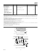
6, 9
Bandwidth –3 dB BW_10 kΩ R
AB
= 10 kΩ 600 kHz
Bandwidth –3 dB BW_50 kΩ R
AB
= 50 kΩ 125 kHz
Bandwidth –3 dB BW_100 kΩ R
AB
= 100 kΩ 71 kHz
Total Harmonic Distortion THD
W
V
A
= 1 V rms, V
B
= 0 V, f = 1 kHz, R
AB
= 10 kΩ 0.003 %
V
W
Settling Time t
S
R
AB
= 10 kΩ/50 kΩ/100 kΩ, ±1 LSB Error Band 2/9/18 µs
Resistor Noise Voltage e
N_WB
R
WB
= 5 kΩ, f = 1 kHz, RS = 0 9 nV√Hz
Crosstalk
10
C
T
V
A
= 5 V, V
B
= 0 V –65 dB