
Datasheet

REV. 0
–3–
AD5207
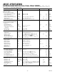
Parameter Symbol Conditions Min Typ
1
Max Unit
INTERFACE TIMING
CHARACTERISTICS
Applies to All Parts
6, 11
Input Clock Pulsewidth t
CH
, t
CL
Clock Level High or Low 10 ns
Data Setup Time t
DS
5ns
Data Hold Time t
DH
5ns
CLK to SDO Propagation Delay
12
t
PD
R
L
= 1 kΩ to 5 V, C
L
< 20 pF 1 25 ns
CS Setup Time t
CSS
10 ns
CS High Pulsewidth t
CSW
10 ns
CLK Fall to CS Fall Hold Time t
CSH0
0ns
CLK Fall to CS Rise Hold Time t
CSH1
0ns
CS Rise to Clock Rise Setup t
CS1
10 ns
NOTES
1
Typicals represent average readings at 25°C and V
DD
= 5 V, V
SS
= 0 V.
2
Resistor position nonlinearity error R-INL is the deviation from an ideal value measured between the maximum resistance and the minimum resistance wiper
positions. R-DNL measures the relative step change from ideal between successive tap positions. Parts are guaranteed monotonic. I
W
= V
DD
/R for both V
DD
= 5 V,
V
SS
= 0 V.
3
V
AB
= V
DD
, Wiper (V
W
) = No connect.
4
INL and DNL are measured at V
W
with the RDAC configured as a potentiometer divider similar to a voltage output D/A converter. V
A
= V
DD
and V
B
= 0 V. DNL
specification limits of ± 1 LSB maximum are Guaranteed Monotonic operating conditions.
5
Resistor Terminals A, B, W have no limitations on polarity with respect to each other.
6
Guaranteed by design and not subject to production test.
7
Measured at the A
X
terminals. All A
X
terminals are open-circuited in shut-down mode.
8
P
DISS
is calculated from (I
DD
× V
DD
). CMOS logic level inputs result in minimum power dissipation.
9
All dynamic characteristics use V
DD
= 5 V, V
SS
= 0 V.
10
Measured at a V
W
pin where an adjacent V
W
pin is making a full-scale voltage change.
11
See timing diagram for location of measured values. All input control voltages are specified with t
R
= t
F
= 2 ns (10% to 90% of 3 V) and timed from a voltage level of
1.5 V. Switching characteristics are measured using V
DD
= 5 V.
12
Propagation delay depends on value of V
DD
, R
L
, and C
L
; see applications text.
The AD5207 contains 474 transistors. Die Size: 67 mil × 69 mil, 4623 sq. mil.
Specifications subject to change without notice.
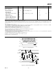
1
0
1
0
1
0
SDI
CLK
CS
V
OUT
RDAC REGISTER LOAD
A1 A0 D7 D6 D5 D4 D3 D2 D1 D0
Figure 1a. Timing Diagram
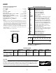
1
0
1
0
1
0
1
0
V
DD
0V
SDI
(DATA IN)
SDO
(DATA OUT)
CLK
CS
V
OUT
Ax OR Dx Ax OR Dx
A'x OR D'x
A
'
x OR D
'
x
ⴞ1LSB ERROR BAND
ⴞ1LSB
t
DS
t
DH
t
PD_MAX
t
CS1
t
CSH1
t
CSW
t
S
t
CL
t
CH
t
CSH0
t
CSS
Figure 1b. Detail Timing Diagram