
Datasheet

REV. 0
AD5207
–4–
CAUTION
ESD (electrostatic discharge) sensitive device. Electrostatic charges as high as 4000 V readily
accumulate on the human body and test equipment and can discharge without detection. Although
the AD5207 features proprietary ESD protection circuitry, permanent damage may occur on
devices subjected to high-energy electrostatic discharges. Therefore, proper ESD precautions are
recommended to avoid performance degradation or loss of functionality.
WARNING!
ESD SENSITIVE DEVICE
ABSOLUTE MAXIMUM RATINGS
1
(T
A
= 25°C, unless otherwise noted)
V
DD
to GND . . . . . . . . . . . . . . . . . . . . . . . . . . . . . . –0.3, +7 V
V
SS
to GND . . . . . . . . . . . . . . . . . . . . . . . . . . . . . . . . . 0, –3 V
V
DD
to V
SS
. . . . . . . . . . . . . . . . . . . . . . . . . . . . . . . . . . . . . 7 V
V
A
, V
B
, V
W
to GND . . . . . . . . . . . . . . . . . . . . . . . . . . V
SS
, V
DD
I
MAX
2
(A, B, W) . . . . . . . . . . . . . . . . . . . . . . . . . . . . . ±20 mA
Digital Inputs and Output Voltage to GND . . 0 V, V
DD
+ 0.3 V
Operating Temperature Range . . . . . . . . . . –40°C to +125°C
Maximum Junction Temperature (T
J
Max) . . . . . . . . . . 150°C
Storage Temperature . . . . . . . . . . . . . . . . . . –65°C to +150°C
Lead Temperature (Soldering, 10 sec) . . . . . . . . . . . . . 300°C
Thermal Resistance
3
θ
JA,
TSSOP-14 . . . . . . . . . . . . . 206°C/W
NOTES
1
Stresses above those listed under Absolute Maximum Ratings may cause perma-
nent damage to the device. This is a stress rating only; functional operation of the
device at these or any other conditions above those indicated in the operational
section of this specification is not implied. Exposure to absolute maximum rating
conditions for extended periods may affect device reliability.
2
Max current is bounded by the maximum current handling of the switches,
maximum power dissipation of the package, and maximum applied voltage
across any two of the A, B, and W Terminals at a given resistance. Please refer to
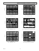
TPC 22 for detail.
3
Package Power Dissipation = (T
J
Max–T
A
)/θ
JA
.
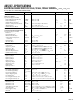
PIN FUNCTION DESCRIPTIONS
Pin Mnemonic Description
1V
SS
Negative Power Supply, specified for opera-
tion from 0 V to –2.7 V.
2 B2 Terminal B of RDAC#2.
3 A2 Terminal A of RDAC#2.
4 W2 Wiper, RDAC#2, addr = 1
2
5 DGND Digital Ground.
6 SHDN Active Low Input. Terminal A open-circuit
and Terminal B shorted to Wiper. Shut-
down controls both RDACs #1 and #2.
7 CS Chip Select Input, Active Low. When CS
returns high, data in the serial input register
is decoded, based on the address bit, and
loaded into the corresponding RDAC register.
8 SDI Serial Data Input. MSB is loaded first.
9 SDO Serial Data Output. Open Drain transistor
requires pull-up resistor.
10 CLK Serial Clock Input. Positive Edge Triggered.
11 V
DD
Positive Power Supply. Specified for opera-
tion at 2.7 V to 5.5 V.
12 W1 Wiper, RDAC #1, addr = 0
2
.
13 A1 Terminal A of RDAC #1.
14 B1 Terminal B of RDAC #1.
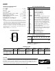
Table I. Serial-Data Word Format
ADDR DATA
B9 B8 B7 B6 B5 B4 B3 B2 B1 B0
A1 A0 D7 D6 D5 D4 D3 D2 D1 D0
MSB LSB
2
9
2
8
2
7
2
0
NOTES
ADDR(RDAC1) = 00; ADDR(RDAC2 = 01).
Data loads B9 first into SDI pin.
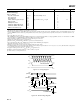
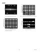
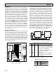
PIN CONFIGURATION
TOP VIEW
(Not to Scale)
14
13
12
11
10
9
8
1
2
3
4
5
6
7
B1
V
SS
AD5207
A1
B2
W1
A2
V
DD
W2
CLK
DGND
SDO
SHDN
SDI
CS
ORDERING GUIDE
Temperature Package Package Qty Per Branding
Model k Range Description Option Container Information*
AD5207BRU10-REEL7 10 –40°C to +125°C TSSOP-14 RU-14 1,000 B10
AD5207BRU50-REEL7 50 –40°C to +125°C TSSOP-14 RU-14 1,000 B50
AD5207BRU100-REEL7 100 –40°C to +125°C TSSOP-14 RU-14 1,000 B100
*Three lines of information appear on the device. Line 1 lists the part number; Line 2 includes branding information and the ADI logo, and Line 3 contains the
date code YYWW.