
Datasheet


AD526
REV. D
–10–
GROUNDING AND BYPASSING
Proper signal and grounding techniques must be applied in
board layout so that specified performance levels of precision
data acquisition components, such as the AD526, are not
degraded.
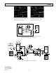
As is shown in Figure 37, logic and signal grounds should be
separate. By connecting the signal source ground locally to the
AD526 analog ground Pins 5 and 6, gain accuracy of the
AD526 is maintained. This ground connection should not be
corrupted by currents associated with other elements within the
system.
GAIN
NETWORK
LATCHES AND LOGIC
DIGITAL
GROUND
AMP
V
OUT
FORCE
V
OUT
SENSE
ANALOG
GROUND 1
ANALOG
GROUND 2
+V
S
–V
S
AD526
V
IN
+15V –15V
0.1mF
0.1mF
0.1mF0.1mF
1mF
+5V
AD574
12-BIT
A/D
CONVERTER
Figure 37. Grounding and Bypassing
OUT
FORCE
OUT
SENSE
0.1mF
–V
S
0.1mF
+V
S
+5V
A2
A1
A0
V
IN
CLK
16 15 14 13 12 11 10 9
12345678
+
–
AD526
168421
GAIN NETWORK
A1 A0 CS CLK A2 B
LOGIC AND LATCHES
OUT
FORCE
OUT
SENSE
V
OUT
0.1mF
–V
S
0.1mF
+V
S
+5V
16 15 14 13 12 11 10 9
12345678
+
–
AD526
168421
GAIN NETWORK
A1 A0 CS CLK A2 B
LOGIC AND LATCHES
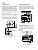
Figure 38. Cascaded Operation
Utilizing the force and sense outputs of the AD526, as shown in
Figure 38, avoids signal drops along etch runs to low impedance
loads.
Table II. Logic Table for Figure 38
V
OUT
/V
IN
A2 A1 A0
1000
2001
4010
8011
16 1 0 0
32 1 0 1
64 1 1 0
128 1 1 1