
Datasheet


Data Sheet AD534
Rev. D | Page 7 of 20
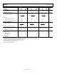
ABSOLUTE MAXIMUM RATINGS
Table 3.
Parameter
AD534J,
AD534K,
AD534L
AD534S,
AD534T
Supply Voltage ±18 V ±22 V
Internal Power Dissipation 500 mW 500 mW
Output Short Circuit to
Ground Indefinite Indefinite
Input Voltages (X
1
, X
2
, Y
1
, Y
2
,
Z
1
, Z
2
) ±V
S
±V
S
Rated Operating
Temperature Range
0°C to +70°C −55°C to +125°C
Storage Temperature
Range −65°C to +150°C −65°C to +150°C
Lead Temperature Range,
60 sec Soldering 300°C 300°C
Stresses above those listed under Absolute Maximum Ratings
may cause permanent damage to the device. This is a stress
rating only; functional operation of the device at these or any
other conditions above those indicated in the operational
section of this specification is not implied. Exposure to absolute
maximum rating conditions for extended periods may affect
device reliability.
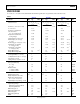
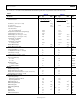
THERMAL RESISTANCE
θ
JA
is specified for the worst-case conditions, that is, a device
soldered in a circuit board for surface-mount packages.
Table 4. Thermal Resistance
Package Type θ
JA
θ
JC
Unit
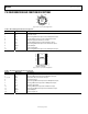
10-Pin TO-100 (H-10) 150 25 °C/W
14-Lead SBDIP (D-14) 95 25 °C/W
20-Terminal LCC (E-20-1) 95 25 °C/W
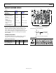
09675-004
Z
1
Z
2
–V
S
+
V
S
Y
2
Y
1
SF
X
2
X
1
OUT
0.076
(1.93)
0.100 (2.54)
5
3
4
8
A
Figure 2. Chip Dimensions and Bonding Diagram
Dimensions shown in inches and (mm)
Contact factory for latest dimensions.
09675-005
+V
S
–V
S
5
0kΩ
1kΩ
TO APPROPRIATE
INPUT TERMINAL
470kΩ
Figure 3. Optional Trimming Configuration
ESD CAUTION