
Datasheet


AD534 Data Sheet
Rev. D | Page 8 of 20
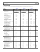
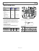
PIN CONFIGURATIONS AND FUNCTION DESCRIPTIONS
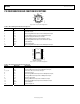
+
V
S
OUT
X1
–V
S
Y1
Y2
SF
X2
Z1
Z2
6
7
8
9
10
3
4
2
1
5
09675-001
AD534
TOP VIEW
(Not to
Scale)
Figure 4. TO-100 (H-10) Pin Configuration
Table 5. H-10 Package Pin Function Descriptions
Pin No. Mnemonic Description
1 X2 Inverting Differential Input of the X Multiplicand Input.
2 SF Scale Factor Input.
3 Y1 Noninverting Differential Input of the Y Multiplicand Input.
4 Y2 Inverting Differential Input of the Y Multiplicand Input.
5 −V
S
Negative Supply Rail. Connects to header.
6 Z2 Inverting Differential Input of the Z Reference Input.
7 Z1 Noninverting Differential Input of the Z Reference Input.
8 OUT Product Output.
9 +V
S
Positive Supply Rail.
10 X1 Noninverting Differential Input of the X Multiplicand Input.
X1
1
X2
2
NC
3
SF
4
+V
S
14
NC
13
OUT
12
Z1
11
NC
5
Z2
10
Y1
6
NC
9
Y2
7
–V
S
8
NC = NO CONNECT. DO NOT
CONNECT TO THIS PIN.
09675-002
AD534
TOP VIEW
(Not to Scale)
Figure 5. TO-100 (D-14) Pin Configuration
Table 6. D-14 Package Pin Function Descriptions
Pin No. Mnemonic Description
1 X1 Noninverting Differential Input of the X Multiplicand Input.
2 X2 Inverting Differential Input of the X Multiplicand Input.
3, 5, 9, 13 NC No Connect. Do not connect to this pin.
4 SF Scale Factor Input.
6 Y1 Noninverting Differential Input of the Y Multiplicand Input.
7 Y2 Inverting Differential Input of the Y Multiplicand Input.
8 −V
S
Negative Supply Rail.
10 Z2 Inverting Differential Input of the Z Reference Input.
11 Z1 Noninverting Differential Input of the Z Reference Input.
12 OUT Product Output.
14 +V
S
Positive Supply rail.