
Datasheet


Data Sheet AD536A
Rev. E | Page 5 of 16
ABSOLUTE MAXIMUM RATINGS
Table 2.
Parameter Rating
Supply Voltage
Dual Supply
±18 V
Single Supply +36 V
Internal Power Dissipation 500 mW
Maximum Input Voltage ±25 V peak
Buffer Maximum Input Voltage ±V
S
Maximum Input Voltage
±25 V peak
Storage Temperature Range
−55°C to +150°C
Operating Temperature Range
AD536AJ/AD536AK 0°C to +70°C
AD536AS −55°C to +125°C
Lead Temperature (Soldering, 60 sec) 300°C
ESD Rating 1000 V
Thermal Resistance θ
JA
1
10-Pin Header (H-10 Package) 150°C/W
20-Terminal LCC (E-20 Package) 95°C/W
14-Lead SBDIP (D-14 Package) 95°C/W
14-Lead CERDIP (Q-14 Package) 95°C/W
Stresses above those listed under Absolute Maximum Ratings
may cause permanent damage to the device. This is a stress
rating only; functional operation of the device at these or any
other conditions above those indicated in the operational
section of this specification is not implied. Exposure to absolute
maximum rating conditions for extended periods may affect
device reliability.
ESD CAUTION
1
θ
JA
is specified for the worst-case conditions, that is, a device soldered in a
circuit board for surface-mount packages.
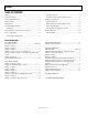
PAD NUMBERS CORRESPOND TO PIN NUMBERS FOR THE
TO-100 14-LEAD CERAMIC DIP PACKAGE.
1
BOTH PADS SHOWN MUST BE CONNECTED TO V
IN
.
THE AD536A IS AVAILABLE IN LASER-TRIMMED CHIP FORM.
SUBSTRATE CONNECTED TO –V
S
.
+V
S
14
V
IN
1A
1
V
IN
1B
1
COM
10
I
OUT
8
BUF IN
7
BUF OUT
6
dB
5
C
AV
4
–V
S
3
R
L
9
0.1315 (3.340)
0.0807
(2.050)
00504-002
Figure 2. Die Dimensions and Pad Layout
Dimensions shown in inches and (millimeters)