
Datasheet


Data Sheet AD536A
Rev. E | Page 13 of 16
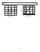
The primary disadvantage in using a large C
AV
to remove ripple
is that the settling time for a step change in input level is
increased proportionately. Figure 19 illustrates that the
relationship between C
AV
and 1% settling time is 115 ms for
each microfarad of C
AV
. The settling time is twice as great for
decreasing signals as it is for increasing signals. The values in
Figure 19 are for decreasing signals. Settling time also increases
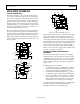
for low signal levels, as shown in Figure 20.
10 100 1k 10k
0.1
1
10
100
0.01
1 100k
INPUT FREQUENCY (Hz)
REQUIRED C
AV
(µF)
0.1
1
10
100
0.01
FOR 1% SETTLING TIME IN SECONDS
MULTIPLY READING BY 0.115
0.01% ERROR
0.1% ERROR
10% ERROR
1% ERROR
1
PERCENT DC ERROR AND PERCENT RIPPLE (PEAK)
VALUES FOR C
AV
AND
1% SETTLING TIME
FOR STATED % OF READING
AVERAGING ERROR
1
ACCURACY ± 20% DUE TO
COMPONENT TOLERANCE
00504-010
Figure 19. Error/Settling Time Graph for Use with the Standard RMS
Connection (See Figure 13 Through Figure 15)
10m 100m 1
7.5
10.0
5.0
1m 10
rms INPUT LEVEL (V)
SETTLING TIME RELATIVE TO 1V rms
INPUT SETTLING TIME
1.0
2.5
00504-011
Figure 20. Settling Time vs. Input Level
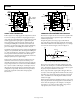
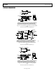
A better method to reduce output ripple is the use of a postfilter.
Figure 21 shows a suggested circuit. If a single-pole filter is used
(C3 removed, R
X
shorted) and C2 is approximately twice the
value of C
AV
, the ripple is reduced, as shown in Figure 22, and
settling time is increased. For example, with C
AV
= 1 µF and C2
= 2.2 μF, the ripple for a 60 Hz input is reduced from 10% of
reading to approximately 0.3% of reading.
The settling time, however, is increased by approximately a
factor of 3. Therefore, the values of C
AV
and C2 can be reduced
to permit faster settling times while still providing substantial
ripple reduction.
The two-pole postfilter uses an active filter stage to provide
even greater ripple reduction without substantially increasing
the settling times over a circuit with a one-pole filter. The values
of C
AV
, C2, and C3 can then be reduced to allow extremely fast
settling times for a constant amount of ripple. Caution should
be exercised in choosing the value of C
AV
, because the dc error
is dependent on this value and is independent of the postfilter.
For a more detailed explanation of these topics, refer to the RMS to
DC Conversion Application Guide, 2nd Edition, available online
from Analog Devices, Inc., at www.analog.com.
C2
V
IN
C
AV
+V
S
14
13
12
11
10
9
8
1
2
3
4
5
6
7
AD536A
25kΩ
ABSOLUTE
VALUE
SQUARER/
DIVIDER
CURRENT
MIRROR
–V
S
Rx
24kΩ
+
–
+
–
C3
1
V
rms
OUT
1
FOR SINGLE POLE, SHORT Rx, REMOVE C3.
00504-012
V
IN
NC
–V
S
C
AV
+V
S
NC
NC
NC
dB
COM
BUF OUT
R
L
BUF IN
I
OUT
BUF
Figure 21. Two-Pole Postfilter
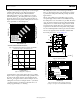
1
1k100 10k
0.1
10
10
DC ERROR OR RIPPLE (% of Reading)
PEAK-TO-PEAK RIPPLE
C
AV
= 1µF
DC ERROR
C
AV
= 1µF
(ALL FILTERS)
PEAK-TO-PEAK RIPPLE
C
AV
= 1µF
C2 = C3 = 2.2µF (TWO-POLE)
00504-013
Rx = 0Ω
PEAK-TO-PEAK
RIPPLE (ONE POLE)
C
AV
= 1µF, C2 = 2.2µF
FREQUENCY (Hz)
Figure 22. Performance Features of Various Filter Types
(See Figure 13 to Figure 15 for Standard RMS Connection)