
Datasheet
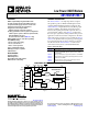


Table Of Contents

AD5700/AD5700-1 Data Sheet
Rev. F | Page 2 of 24
TABLE OF CONTENTS
Features .............................................................................................. 1
Applications ....................................................................................... 1
General Description ......................................................................... 1
Functional Block Diagram .............................................................. 1
Revision History ............................................................................... 2
Specifications ..................................................................................... 3
Timing Characteristics ................................................................ 5
Absolute Maximum Ratings ............................................................ 6
Thermal Resistance ...................................................................... 6
ESD Caution .................................................................................. 6
Pin Configuration and Function Descriptions ............................. 7
Typical Performance Characteristics ............................................. 9
Terminology .................................................................................... 12
Theory of Operation ...................................................................... 13
FSK Modulator ........................................................................... 13
Connecting to HART_OUT ..................................................... 14
FSK Demodulator ...................................................................... 14
Connecting to HART_IN or ADC_IP .................................... 14
Clock Configuration .................................................................. 15
Supply Current Calculations ..................................................... 16
Power-Down Mode .................................................................... 16
Full Duplex Operation ............................................................... 16
Applications Information .............................................................. 17
Supply Decoupling ..................................................................... 17
Transient Voltage Protection .................................................... 17
Typical Connection Diagrams .................................................. 18
Outline Dimensions ....................................................................... 21
Ordering Guide .......................................................................... 21
REVISION HISTORY
1/14—Rev. E to Rev. F
Changes to Figure 3 to Figure 7 ...................................................... 9
Changes to Example Section ......................................................... 14
10/13—Rev. D to Rev. E
Changes to t
7
and t
8
Descriptions, Table 3 ..................................... 5
Changed θ
JA
from 30°C/W to 56°C/W .......................................... 6
Added Figure 13 and Figure 14 .................................................... 10
Changes to External Crystal Section and Figure 25 .................. 15
5/13—Rev. C to Rev. D
2/13—Rev. B to Rev. C
Changed 2 V to 5.5 V Power Supply to 1.71 V to 5.5 V Power
Supply, Features Section .................................................................. 1
Changes to Summary Statement, V
CC
Parameter, and Internal
Reference Voltage Parameter Test Conditions/Comments,
Table 2 ................................................................................................ 3
Changed V
CC
= 2 V to 5.5 V to V
CC
= 1.71 V to 5.5 V in the
Summary Statement, Table 3 ........................................................... 5
Changes to Pin 18 Description and EPAD Mnemonic and
Description, Table 6 .......................................................................... 7
Changes to Figure 9 and Figure 13 ............................................... 10
Changes to Figure 28 ...................................................................... 18
Change to Figure 30 ....................................................................... 20
7/12—Rev. A to Rev. B
Removed V
CC
and IOV
CC
Current Consumption Text, Table 2 .. 3
Added Internal Oscillator and External Clock Parameters
to Table 2 ............................................................................................. 4
Changes to t
2
Description and Endnote 2, Table 3........................ 5
Changes to IOV
CC
Description, Table 6 .......................................... 7
Added Supply Current Calculations Section .............................. 16
Added Transient Voltage Protection Section, Figure 26, and
Figure 27; Renumbered Sequentially ........................................... 17
Changes to Typical Connection Diagrams Section ................... 18
Changes to Figure 29...................................................................... 19
Changes to Figure 30...................................................................... 20
Updated Outline Dimensions ....................................................... 21
4/12—Rev. 0 to Rev. A
Change to Transmit Impedance Parameter,
RTS
Low, Table 2 ... 4
Changes to Figure 3, Figure 4, Figure 5, and Figure 7 .................. 9
Changes to Figure 10 and Figure 11 ............................................ 10
Changed AD5755 to AD5755-1 Throughout ............................. 17
Change to Figure 27 ....................................................................... 18
2/12—Revision 0: Initial Version