
Datasheet


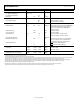


Table Of Contents

Data Sheet AD5700/AD5700-1
Rev. F | Page 5 of 24
TIMING CHARACTERISTICS
V
CC
= 1.71 V to 5.5 V, IOV
CC
= 1.71 V to 5.5 V, T
MIN
to T
MAX
, unless otherwise noted.
Table 3.
Parameter
1
Limit at T
MIN
, T
MAX
Unit Description
t
1
1 Bit time
2
max Carrier start time. Time from
RTS
falling edge to carrier reaching its first peak. See
Figure 3.
t
2
1 Bit time
2
max Carrier stop time. Time from
RTS
rising edge to carrier amplitude dropping below
the minimum receive amplitude.
t
3
1 Bit time
2
max Carrier decay time. Time from
RTS
rising edge to carrier amplitude dropping to ac
zero. See Figure 4.
t
4
6 Bit times
2
max Carrier detect on. Time from carrier on to CD rising edge. See Figure 5.
t
5
6 Bit times
2
max Carrier detect off. Time from carrier off to CD falling edge. See Figure 6.
t
6
10 Bit times
2
max Carrier detect on when switching from transmit mode to receive mode in the
presence of a constant valid carrier. Time from
RTS
rising edge to CD rising edge.
See Figure 7.
t
7
2.1 ms typ Crystal oscillator power-up time. On application of a valid power supply voltage at
V
CC
or on enabling of the oscillator via the
XTAL_EN
pin. Crystal load capacitors =
16 pF.
t
8
6 ms typ Crystal oscillator power-up time. Crystal load capacitors = 36 pF.
t
9
25 µs typ Internal oscillator power-up time. On application of a valid power supply voltage
at V
CC
or on enabling of the oscillator via the CLK_CFG0 and CLK_CFG1 pins.
t
10
10 ms typ Reference power-up time.
t
11
30 µs typ Transition time from power-down mode to normal operating mode (external
clock source, external reference).
1
Specifications apply to AD5700/AD5700-1 configured with internal or external receive filter.
2
Bit time is the length of time to transfer one bit of data (1 bit time = 1/1200 Hz = 833.333 µs).