
Datasheet


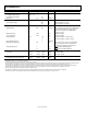


Table Of Contents

Data Sheet AD5700/AD5700-1
Rev. F | Page 7 of 24
PIN CONFIGURATION AND FUNCTION DESCRIPTIONS
Figure 2. Pin Configuration
Table 6. Pin Function Descriptions
Pin No. Mnemonic Description
1
XTAL_EN
Crystal Oscillator Circuit Enable. A low state enables the crystal oscillator circuit, and an external crystal is
required. A high state disables the crystal oscillator circuit, and an external clock source or the internal oscillator
(AD5700-1only) provides the clock source. This pin is used in conjunction with the CLK_CFG0 and CLK_CFG1 pins
in configuring the required clock generation scheme.
2 CLKOUT
Clock Output. If using the crystal oscillator or the internal RC oscillator, a clock output can be configured at the
CLKOUT pin. Enabling the clock output consumes extra current to drive the load on this pin. See the CLKOUT
section for more details.
3 CLK_CFG0 Clock Configuration Control. See Table 7.
4 CLK_CFG1 Clock Configuration Control. See Table 7.
5
RESET
Active Low Digital Input. Holding RESET low places the AD5700/AD5700-1 in power-down mode. A high state on
RESET returns the AD5700/AD5700-1 to their power-on state. If not using this pin, tie this pin to IOV
CC
.
6 CD Carrier Detect—Digital Output. A high on CD indicates a valid carrier is detected.
7 TXD Transmit Data—Digital Input. Data input to the modulator.
8
RTS
Request to Send—Digital Input. A high state enables the demodulator and disables the modulator. A low state
enables the modulator and disables the demodulator.
9 DUPLEX
A high state on this pin enables full duplex operation. See the Theory of Operation section. A low state disables
this feature.
10 RXD Receive Data—UART Interface Digital Data Output. Data output from the demodulator is accessed on this pin.
11 IOV
CC
Digital Interface Supply. Digital threshold levels are referenced to the voltage applied to this pin. The applied
voltage can be in the range of 1.71 V to 5.5 V. IOV
CC
should be decoupled to ground with low ESR 10 μF and
0.1 μF capacitors (see the Supply Decoupling section).
12 DGND
Digital Circuitry Ground Reference Connection. For typical operation, it is recommended to connect this pin to
AGND.
13 REG_CAP Capacitor Connection for Internal Voltage Regulator. Connect a 1 μF capacitor from this pin to ground.
14 HART_OUT HART FSK Signal Output. See the FSK Modulator section and Figure 30 for typical connections.
15 REF
Internal Reference Voltage Output, or External 2.5 V Reference Voltage Input. Connect a 1 μF capacitor from this
pin to ground. When supplying an external reference, the V
CC
supply requires a minimum voltage of 2.7 V.
16 HART_IN
HART FSK Signal. When using the internal filter, couple the HART input signal into this pin using a 2.2 nF series
capacitor. If using an external band-pass filter as shown in Figure 23, do not connect to this pin.
17 ADC_IP
If using the internal band-pass filter, connect 680 pF to this pin. Alternatively, this pin allows direct connection to
the ADC input, in which case an external band-pass filter network must be used, as shown in Figure 23.
18 V
CC
Power Supply Input. 1.71 V to 5.5 V can be applied to this pin. V
CC
should be decoupled to ground with low ESR
10 μF and 0.1 μF capacitors (see the Supply Decoupling section).
10435-002
NOTES
1. THE EXPOSED
PADDLE SHOULD BE CONNECTED
TO
AGN
D OR DGND, OR, ALTERNATIVELY, IT CA
N
B
E LEFT ELEC
TRICALLY UNCONNECTED.
IT IS
RECOMMENDED THAT THE PADDLE
BE THERMALLY
CONNECTED
TO A COPPER PL
ANE
FOR ENHANCED
THERMAL PERFORMANC
E.
2
1
3
4
5
6
18
17
16
15
14
13
CD
RESET
CLK_CFG1
C
LK_CFG0
CLKOUT
X
TAL_EN
REG_CAP
HART
_OUT
REF
HAR
T_IN
ADC_IP
V
CC
8
9
10
11
7
R
TS
DUPLEX
RXD
IOV
CC
12
DGND
TXD
20
19
21
XTAL2
AGND
XTAL1
22
DGND
23
REF_EN
24
FILTER_SEL
AD5700/
AD5700-1
TOP VIEW
(Not to Scale)