
Datasheet


AD580
Rev. B | Page 4 of 8
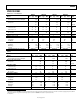
ABSOLUTE MAXIMUM RATINGS
Table 3.
Parameter Rating
Input Voltage 40 V
Power Dissipation @ 25°C
Ambient Temperature 350 mW
Derate above 25°C 2.8 mW/°C
Lead Temperature (Soldering
10 sec)
300°C
Thermal Resistance
Junction-to-Case 100°C
Junction-to-Ambient 360°C/W
Stresses above those listed under Absolute Maximum Ratings
may cause permanent damage to the device. This is a stress
rating only; functional operation of the device at these or any
other conditions above those listed in the operational sections
of this specification is not implied. Exposure to absolute
maximum rating conditions for extended periods may affect
device reliability.
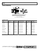
AD580 CHIP DIMENSIONS AND PAD LAYOUT
Dimensions shown in inches and (millimeters).
00525-B-002
*BOTH E
OUT
PADS MUST BE CONNECTED TO THE OUTPUT.
0.075 (1.90)
E
OUT
*
–E
+E
0.046
(1.16)
Figure 2.
The AD580 is also available in chip form. Consult the factory
for specifications and applications information.
ESD CAUTION
ESD (electrostatic discharge) sensitive device. Electrostatic charges as high as 4000 V readily accumulate on
the human body and test equipment and can discharge without detection. Although this product features
proprietary ESD protection circuitry, permanent damage may occur on devices subjected to high energy
electrostatic discharges. Therefore, proper ESD precautions are recommended to avoid performance
degradation or loss of functionality.