
Datasheet


AD580
Rev. B | Page 5 of 8
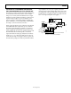
THEORY OF OPERATION
The AD580 family (AD580, AD581, AD584, AD589) uses the
bandgap concept to produce a stable, low temperature coef-
ficient voltage reference suitable for high accuracy data acqui-
sition components and systems. The device makes use of the
underlying physical nature of a silicon transistor base-emitter
voltage in the forward-biased operating region. All such tran-
sistors have approximately a –2 mV/°C temperature coefficient,
unsuitable for use directly as a low TC reference. Extrapolation
of the temperature characteristic of any one of these devices to
absolute zero (with an emitter current propor-tional to the
absolute temperature), however, reveals that it will go to a V
BE
of
1.205 V at 0 K, as shown in Figure 3. Thus, if a voltage could be
developed with an opposing temperature coefficient to sum
with V
BE
to total 1.205 V, a 0 TC reference would result and
operation from a single, low voltage supply would be possible.
The AD580 circuit provides such a compensating voltage, V1 in
Figure 4, by driving two transistors at different current densities
and amplifying the resulting V
BE
difference (∆V
BE
—which now
has a positive TC). The sum, V
Z
, is then buffered and amplified
up to 2.5 V to provide a usable reference-voltage output. Figure
5 shows the schematic diagram of the AD580.
The AD580 operates as a 3-terminal reference, meaning that no
additional components are required for biasing or current
setting. The connection diagram, Figure 6, is quite simple.
1.5
1.0
1.205
0.5
0
–273°C –200°C –100°C 100°C0°C
0K 73K 173K 373K273K
00525-B-003
TEMPERATURE
JUNCTION VOLTAGE (V)
FOR BOTH
DEVICES
REQUIRED
COMPENSATION
VOLTAGE–
SAME DEVICES
V
BE
VS. TEMPERATURE
FOR TWO TYPICAL
DEVICES (I
E
α
T)
CONSTANT SUM = 1.205V
Figure 3. Extrapolated Variation of Base-Emitter Voltage with Temperature
(I
E
αT), and Required Compensation, Shown for Two Different Devices
00525-B-004
R7R8
R2
R1
I
2
≅
I
1
2I
1
= I
1
+ I
2
+V
IN
COM
R4
R5
Q2
8A
Q1
A
V
1
= 2
∆
V
BE
R
1
R
2
∆
V
BE
V
BE
(Q1)
V
OUT
= V
Z
1 + = 2.5V
R
4
R
5
= V
BE
+ 2
∆
V
BE
R
1
R
2
= V
BE
+ 2 ln
R
1
R
2
kT
q
J
1
J
2
= 1.205V
V
Z
= V
BE
+ V
1
Figure 4. Basic Bandgap-Reference Regulator Circuit
00525-B-005
COM
R12 R13
R7
Q14
Q3
Q13
Q7
Q4
Q10 Q11
Q12
Q15
Q5
Q6
Q8
Q9
Q2
8A
Q1
A
R2
R1
R3
R6
C1
R11
R5
R4
R9
R10
R8
–E
+E
2.5V
OUT
Figure 5. Schematic Diagram
00525-B-006
+E
4.5
≤
V
IN
≤
30V
–E
E
OUT
LOAD
AD580
Figure 6. Connection Diagram
VOLTAGE VARIATION VERSUS TEMPERATURE
Some confusion exists in the area of defining and specifying
reference voltage error over temperature. Historically, references
are characterized using a maximum deviation per degree
Centigrade; i.e., 10 ppm/°C. However, because of the
inconsistent nonlinearities in Zener references (butterfly or S
type characteristics), most manufacturers use a maximum limit
error band approach to characterize their references. This
technique measures the output voltage at 3 to 5 different
temperatures and guarantees that the output voltage deviation
will fall within the guaranteed error band at these discrete
temperatures. This approach, of course, makes no mention or
guarantee of performance at any other temperature within the
operating temperature range of the device.