
Datasheet


AD581
Rev. C | Page 7 of 12
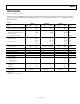
The error band which is guaranteed with the AD581 is the
maximum deviation from the initial value at +25°C; this error
band is of more use to a designer than one which simply guarantees
the maximum total change over the entire range (that is, in the
latter definition, all of the changes could occur in the positive
direction). Thus, with a given grade of the AD581, the designer
can easily determine the maximum total error from initial toler-
ance plus temperature variation (for example, for the AD581T, the
initial tolerance is ±10 mV, the temperature error band is ±15 mV,
thus the unit is guaranteed to be 10.000 V ±25 mV from −55°C
to +125°C).
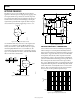
OUTPUT CURRENT CHARACTERISTICS
The AD581 has the capability to either source or sink current
and provide good load regulation in either direction, although
it has better characteristics in the source mode (positive current
into the load). The circuit is protected for shorts to either positive
supply or ground. The output voltage vs. output current charac-
teristics of the device are shown in Figure 6. Source current
is displayed as negative current in the figure; sink current is
positive. Note that the short-circuit current (that is, 0 V output)
is about 28 mA; when shorted to +15 V, the sink current goes to
about 20 mA.
–20 –15 –10 –5 0 5 10 15 20
14
12
10
8
6
4
2
0
OUTPUT VOLTAGE (V)
OUTPUT CURRENT (mA)
SOURCE SINK
+V
S
= 15V
T
A
= 25°C
08014-006
Figure 6. Output Voltage vs. Sink and Source Current
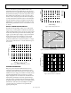
DYNAMIC PERFORMANCE
Many low power instrument manufacturers have been in-
creasingly concerned with the turn-on characteristics of the
components used in their systems. Fast turn-on components often
enable the end user to keep power off when not needed, and yet
respond quickly when the power is turned on for operation.
Figure 7 displays the turn-on characteristic of the AD581. This
characteristic is generated from a cold start operation and repre-
sents the true turn-on waveform after an extended period with
the supplies off. The figure shows both the coarse and fine transient
characteristics of the device; the total settling time to within
±10 mV is about 180 s, and there is no long thermal tail
appearing after the point.
0 50 100 150 200 250
12
V
11V
10V
20V
10V
0V
10.03V
OUTPUT
10.02V
10.01V
10.00V
SETTLING TIME (µs)
OUTPUTINPUT
08014-007
Figure 7. Output Settling Characteristic
1000
1
10 1M
FREQUENCY (Hz)
100 1k 10k 100k
10
100
NOISE SPECTRAL DENSITY (nV/ Hz)
TOTAL NOISE (µV rms) UP
TO SPECIFIED FREQUENCY
08014-008
Figure 8. Spectral Noise Density and Total rms Noise vs. Frequency
1000
500
TEMPERATURE (°C)
SUPPLY CURRENT (µA)
–50–55 –40 –30 –20 –10 0 10 20 30 40 50 60 70 80 90 100 110 120 125
900
800
700
600
1.5µA/°C
08014-009
Figure 9. Quiescent Current vs. Temperature