
Datasheet

AD587
Rev. H | Page 10 of 12
APPLICATIONS INFORMATION
USING THE AD587 WITH CONVERTERS
The AD587 is an ideal reference for a variety of 8-bit, 12-bit,
14-bit, and 16-bit ADCs and DACs. Several examples follow.
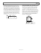
10 V Reference with Multiplying CMOS DACs or ADCs
The AD587 is ideal for applications with 10-bit and 12-bit
multiplying CMOS DACs. In the standard hookup, shown in
Figure 18, the AD587 is paired with the AD7545 12-bit multi-
plying DAC and the
AD711 high speed BiFET op amp. The
amplifier DAC configuration produces a unipolar 0 V to −10 V
output range. Bipolar output applications and other operating
details can be found in the individual product data sheets.
AD587
GND
AD711
–15V
+15V
OUT1
DGND
DB11 TO DB0
C1
33pF
R2
+15V
AD7545
TRIM
+15
V
+V
IN
V
OUT
0.1µF
V
REF
V
DD
R
FB
AGND
0.1µF
0.1µF
V
OUT
0V TO –10V
00530-019
10kΩ
Figure 18. Low Power 12-Bit CMOS DAC Application
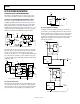
The AD587 can also be used as a precision reference for multi-
ple DACs.
Figure 19 shows the AD587, the AD7628 dual DAC,
and the
AD712 dual op amp hooked up for single-supply
operation to produce 0 V to −10 V outputs. Because both DACs
are on the same die and share a common reference and output
op amps, the DAC outputs will exhibit similar gain temperature
coefficients (TCs).
AD587
GND
AD712
+15V
OUT A
DGND
+15V
AGND
DAC A
DB0
DB7
OUT B
DAC B
18
RFB B
RFB A
AD7628
+V
IN
V
OUT
0.1µF
DATA
INPUTS
V
REF
A
V
REF
B
V
OUT
A =
0 TO –10V
V
OUT
B =
0 TO –10V
0
0530-020
Figure 19. AD587 as a 10 V Reference for a CMOS Dual DAC
Precision Current Source
The design of the AD587 allows it to be easily configured as a cur-
rent source. By choosing the control resistor (R
C
) via the equation
shown in
Figure 20, the user can vary the load current from the
quiescent current (2 mA typically) to approximately 10 mA.
2
6
4
GND
AD587
+
V
IN
+V
IN
V
OUT
I
L
= + I
BIAS
10V
R
C
R
C
500Ω
MIN
00530-021
Figure 20. Precision Current Source
Precision High Current Supply
For higher currents, the AD587 can easily be connected to a
power PNP or power Darlington PNP device. The circuits in
Figure 21 and Figure 22 can deliver up to 4 A to the load. The
0.1 µF capacitor is required only if the load has a significant
capacitive component. If the load is purely resistive, improved
high frequency supply rejection results can be obtained by
removing the capacitor.
AD587
2
6
4
2N6285
R
C
V
OUT
I
L
= + I
BIAS
10V
R
C
00530-022
+V
IN
0.1µF
+
V
IN
220Ω
GND
Figure 21. Precision High Current Source
AD587
2
6
4
2N6285
V
OUT
+V
IN
0.1µF
+
V
IN
220Ω
V
OUT
+10V @ 4A
00530-023
GND
Figure 22. Precision High Current Voltage Source