
Datasheet

AD587
Rev. H | Page 5 of 12
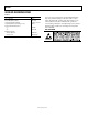
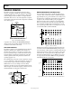
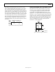
PIN CONFIGURATION AND FUNCTION DESCRIPTIONS
1
2
3
4
8
7
6
5
AD587
TOP VIEW
(Not to Scale)
TRIM
V
OUT
TP*
NOISE
REDUCTION
+V
IN
GND
TP*
TP*
*TP DENOTES FACTORY TEST POINT.
NO CONNECTIONS SHOULD BE MADE
TO THESE PINS.
00530-002
Figure 2. Pin Configuration
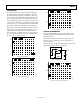
Table 3. Pin Function Descriptions
Pin No. Mnemonic Description
1, 3, 7 TP No Connection. Leave floating.
2 +V
IN
Input Voltage.
4 GND Ground.
5 TRIM Fine Trimming of Output Voltage. See Figure 4.
6 V
OUT
Output Voltage.
8 NOISE REDUCTION Noise Reduction of Output Voltage. Reduces noise via external capacitor to ground.