
Datasheet

AD587
Rev. H | Page 7 of 12
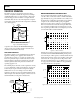
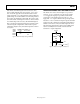
TURN-ON TIME
Upon application of power (cold start), the time required for
the output voltage to reach its final value within a specified
error band is defined as the turn-on settling time. Two compo-
nents normally associated with this are the time for the active
circuits to settle and the time for the thermal gradients on the
chip to stabilize.
Figure 7, Figure 8, and Figure 9 show the turn-
on characteristics of the AD587. These figures show the settling
to be about 60 µs to 0.01%. Note the absence of any thermal tails
when the horizontal scale is expanded to 1 ms/cm in
Figure 8.
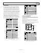
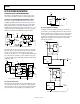
Output turn-on time is modified when an external noise reduc-
tion capacitor is used. When present, this capacitor acts as an
additional load to the current source of the internal Zener
diode, resulting in a somewhat longer turn-on time. In the case
of a 1 µF capacitor, the initial turn-on time is approximately
400 ms to 0.01%, as shown in
Figure 9.
100
10
0%
10V
1mV
90
+V
IN
V
OUT
20µs
00530-007
Figure 7. Electrical Turn-On
100
90
10
0%
10V
1ms
20V
+V
IN
V
OUT
0
0530-008
Figure 8. Extended Time Scale
100
90
10
0%
1V
100ms
10V
+V
IN
V
OUT
00530-009
Figure 9. Turn-On with 1 μF C
N
DYNAMIC PERFORMANCE
The output buffer amplifier is designed to provide the AD587
with static and dynamic load regulation that is superior to less
complete references.
Many ADCs and DACs present transient current loads to the
reference, and poor reference response can degrade the con-
verter’s performance.
Figure 11 and Figure 12 display the characteristics of the AD587
output amplifier driving a 0 mA to 10 mA load.
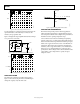
00530-010
AD587
V
OUT
7.0V
1kΩ
10V
0V
V
L
Figure 10. Transient Load Test Circuit
100
90
10
0%
50mV 1µs10V
V
L
V
OUT
0
0530-011
Figure 11. Large-Scale Transient Response