
Datasheet

AD587
Rev. H | Page 8 of 12
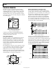
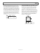
100
90
10
0%
1mV 2µs10V
V
L
V
OUT
00530-012
Figure 12. Fine-Scale Setting for Transient Load
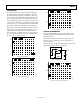
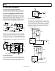
In some applications, a varying load may be both resistive and
capacitive in nature, or the load may be connected to the
AD587 by a long capacitive cable.
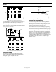
Figure 14 displays the output amplifier characteristics driving a
1000 pF, 0 mA to 10 mA load.
AD587
V
OUT
7.0V
1kΩ
V
L
10V
0V
C
L
1000pF
00530-013
Figure 13. Capacitive Load Transient/Response Test Circuit
100
90
10
0%
200mV 1µs10V
C
L
= 0
C
L
= 1000pF
V
L
00530-014
Figure 14. Output Response with Capacitive Load
LOAD REGULATION
The AD587 has excellent load regulation characteristics.
Figure 15 shows that varying the load several milliamperes
changes the output by only a few microvolts.
–6 –4 –2 0
–500
–1000
500
1000
Δ
V
OUT
(µV)
LOAD (mA)
24 6810
00530-015
Figure 15. Typical Load Regulation Characteristics
TEMPERATURE PERFORMANCE
The AD587 is designed for precision reference applications
where temperature performance is critical. Extensive tempera-
ture testing ensures that the device’s high level of performance is
maintained over the operating temperature range.
Some confusion exists in the area of defining and specifying
reference voltage error over temperature. Historically, references
have been characterized using a maximum deviation per degree
Celsius, such as ppm/°C. However, because of nonlinearities in
temperature characteristics that originated in standard Zener
references (such as S-type characteristics), most manufacturers
have begun to use a maximum limit error-band approach to
specify devices. This technique involves the measurement of the
output at three or more temperatures to specify an output
voltage error band.